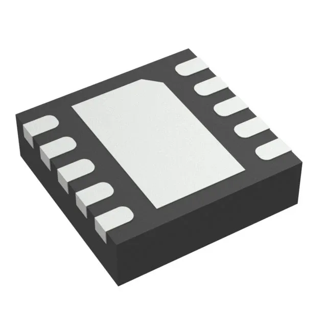
Dual-rail supply in a 3x3 mm footprint
One channel is rated for 400 mA, the other for 600 mA continuous output — a pairing sized for a low-power SoC core (1.1 V) and its I/O or analog rail (1.575 V or 2.8 V) in a single 10-VSON package.
Switching at 2.25 MHz — inductor sizing trade-off
The 2.25 MHz switching frequency lets you use 1 µH to 2.2 µH inductors and small ceramic output capacitors, shrinking the total solution footprint. The trade-off is higher switching losses at light load — expect efficiency to peak above 90% at moderate loads and drop off below 10 mA load. For battery-powered designs where light-load efficiency matters, evaluate the PFM mode behaviour in the datasheet. Both outputs use synchronous rectification, so no external Schottky catch diode is needed. That saves a component and keeps the layout tighter, but the bottom FET's dead-time control sets the efficiency floor at very light loads.
Industrial temperature, not automotive qualified
It is not AEC-Q100 qualified, so do not route it into an under-hood or cabin automotive power tree without a waiver. The supplier device package is 10-VSON (3x3); the PCB land pattern should match the TI recommended footprint in the datasheet.
The TPS62403DRCT is the tape-and-reel variant (2,500/reel); the cut-tape option is also listed for prototype or small-run quantities.