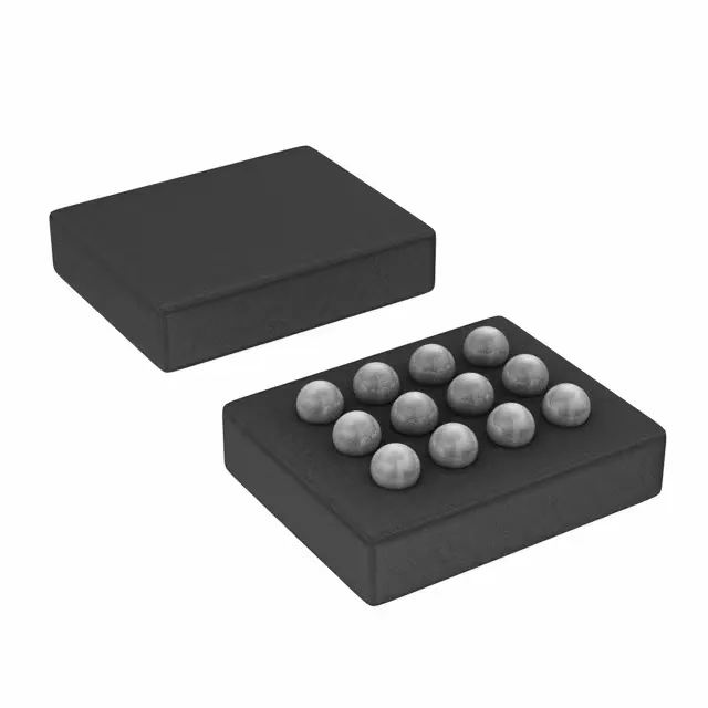
Package and board integration — 12-bump DSBGA
The TPS62350YZGT comes in a 12-bump DSBGA (12-UFBGA) package, a fine-pitch wafer-level chip-scale package with no leads — the bumps are the only interface to the board. This means the footprint is essentially the die size plus a fan-out ring; the 0.50 mm pitch demands a PCB with at least two signal layers and a via-in-pad approach for the centre bumps. The supplier device package is 12-DSBGA, identical to the case code. Because the DSBGA lacks a moulded body, the silicon backside is exposed after reflow — handle the parts with vacuum pick-and-place only; tweezers will chip the die edge.
What the 3 MHz switching frequency means for your rail design
The trade-off is that switching losses scale with frequency; at 800 mA load the efficiency peaks around 90% at 3.6 V input, but drops to the mid-80s at 5.5 V input due to the higher gate-drive loss in the internal FETs. The 3 MHz switching also pushes the fundamental switching noise above the AM radio band, which simplifies filtering in RF-sensitive designs — a BLE or Wi-Fi module on the same board will see less conducted spurious at the carrier frequency than with a 1 MHz switcher. The synchronous rectifier helps maintain efficiency at light loads by replacing the freewheeling diode with a low-Rds(on) FET.
Output voltage flexibility — adjustable or preset
The TPS62350 offers an adjustable output from 0.75 V up to 1.54 V via an external resistor divider, but also includes factory-programmable preset voltages at 1.05 V and 1.35 V — these are selected by a logic pin, not by resistor values. For a fixed-rail design like a 1.2 V core supply, the preset option saves two feedback resistors and one bypass cap on the feedback node. The output configuration is positive, so it's a standard buck — no inverting or SEPIC topology. The minimum output of 0.75 V means it can power low-voltage digital cores down to the 0.8 V range, but not sub-0.7 V rails used in some advanced FinFET ASICs.
Active production and compliance documentation
Texas Instruments provides a datasheet with full electrical characteristics, application notes for layout guidelines, and an evaluation module (EVM) user guide.