That means official factory support has ended — no last-time-buy window remains open through the franchised channel.
3 MHz switching — what it buys the layout
The 3 MHz switching frequency lets the output filter use a physically small inductor — typically in the 1 µH range — which shrinks the total solution footprint. Switching losses scale with frequency, so efficiency at light loads is lower than a 1 MHz regulator. The synchronous rectifier helps, but the thermal budget in the 8-DSBGA package still needs the copper pour on the PCB to pull heat out.
Output current and voltage range — sizing the rail
Rated 500 mA continuous output, adjustable from 0.6 V up to 5.4 V. The 500 mA ceiling means it fits a local point-of-load rail for a sensor, RF transceiver, or low-power MCU — not a system-level power bus.
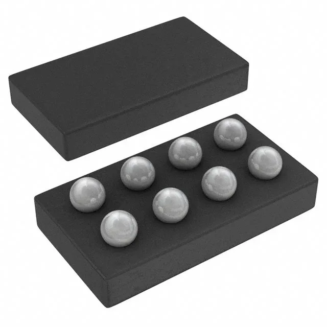
The 8-pin DSBGA is a wafer-level chip-scale package. The solder balls are under the die, so the PCB land pattern must match TI's recommended layout exactly — no scope for hand-routing between pads.