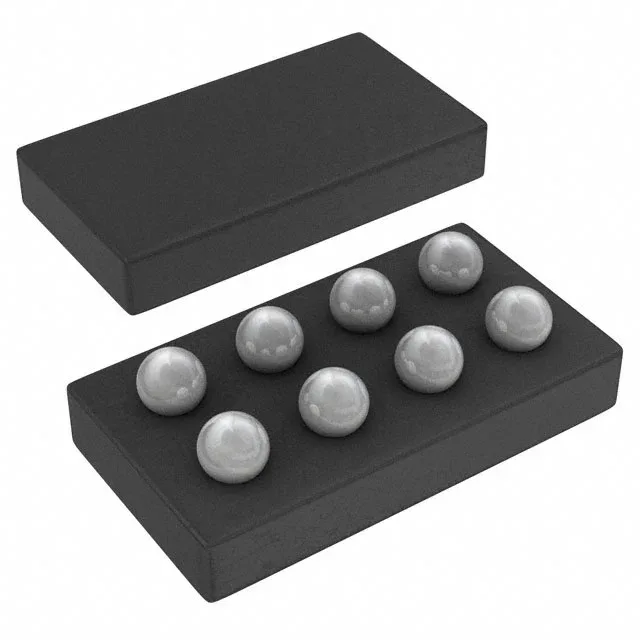
The TPS62313YZDR: The 3 MHz switching frequency lets you use small 1 µH inductors and 4.7 µF ceramic output capacitors, shrinking the total solution footprint to fit under 15 mm² on a single-sided PCB. The output is factory-set to 1.8 V (fixed), so no external feedback divider is needed — the BOM count stays low. Synchronous rectification (internal low-side FET) eliminates the external Schottky diode and improves efficiency above 85% across the load range.
Obsolete — sourcing and replacement planning
For new designs, TI's TPS62313 family shares the same pinout and 8-DSBGA footprint across output voltage options (0.8 V to 1.8 V fixed), but a direct pin-compatible replacement with identical 500 mA / 3 MHz rating is not formally cross-referenced. Evaluate the TPS62313YZDR's 1.8 V fixed output against the TPS62313 series voltage variants if the board layout and inductor can accommodate a slightly different output set-point.
Package and layout — 8-DSBGA realities
The 3 MHz switching edge rate means the input capacitor (4.7 µF ceramic, 0805 or smaller) must sit within 2 mm of the VIN ball to keep switching noise below 50 mVpp.