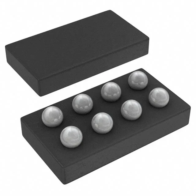
Package and footprint — the fit constraint
This part comes in an 8-pin DSBGA (8-UFBGA) package, a tiny 0.4 mm pitch wafer-level chip-scale package. The 8-DSBGA supplier device package is the same footprint. Any replacement candidate must be pin-compatible or the board layout changes. The surface-mount DSBGA package is not suited for hand-soldering or rework without a hot-air station and stencil. The scorch mark on a dead board often points to a cracked solder ball under the package rather than a failed die.
The 3 MHz switching frequency is relatively high, which lets the converter use small inductors and capacitors, but it also means the replacement must have a similar frequency range to keep the output ripple and transient response in the same ballpark. The 500 mA output current and 2.7 V to 6 V input range set the power budget. A replacement with lower current or narrower input range won't work; one with higher current may be overkill but still fit if the package matches. The fixed 1.8 V output and positive output configuration mean the regulator is not adjustable — any replacement must also output 1.8 V fixed, or the feedback network on the board must be changed.