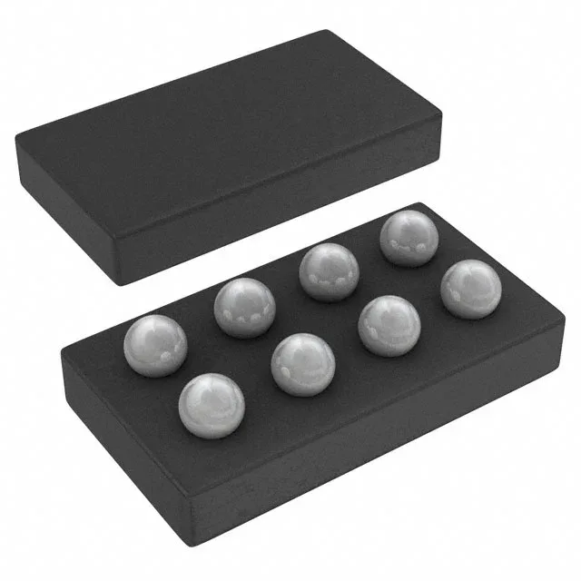
3 MHz buck in an 8-bump DSBGA — what that means for a tight board
The TPS62300YZDT: The output is adjustable from 0.6 V up to 5.4 V, which covers the core and I/O voltages for most low-power MCUs, FPGAs, and RF chipsets. The 3 MHz switching frequency pushes the inductor and capacitor values down — a 1 µH to 2.2 µH inductor and 10 µF ceramic output cap are typical — so the total solution fits in roughly the footprint of the DSBGA package itself. The 8-bump DSBGA (0.5 mm pitch, no leadframe) is the smallest footprint option for this current class, but it demands a controlled SMT process — the solder mask opening and stencil aperture need to match the TI layout recommendation to avoid head-in-pillow and cold-joint defects. The synchronous rectifier is integrated, so no external Schottky catch diode is needed; that saves one component and one placement step.
Obsolete — no official drop-in replacement on record
There is no official TI successor order code listed for this exact DSBGA variant. For a BOM that needs this footprint and pinout, the realistic path is to qualify a functionally equivalent part from a different package family and respin the board layout.
Industrial temp range and the sourcing picture
Sourcing this obsolete part is a spot-market play. If you are buying for a repair or short-run production, confirm the date code and bake condition before reflow.