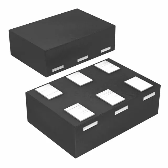
500 mA in a 1.45x1 mm SON — the thermal and load budget
The TPS62239DRYR is a fixed 1 V output, 500 mA step-down converter from Texas Instruments, switching at 3 MHz to shrink the inductor and output capacitors down to 0603 or 0402 case sizes. The 6-pin SON package (1.45 mm x 1 mm) is the smallest footprint in the TPS6223x family, but the thermal pad is correspondingly small — at 500 mA continuous from a 5 V input, the junction rise above ambient is roughly 40-50°C, so the full 125°C rating is only usable if the board copper area under the pad is generous.
Input voltage range — the common BOM trap
The input range is 2.05 V to 6 V. That 2.05 V minimum lets it run from a single Li-ion cell down to its discharge floor, but the 6 V maximum means it cannot be used on a 12 V or 24 V industrial rail — a mistake that shows up when a designer grabs a 'small buck' without checking the abs-max. If the input bus is above 6 V, step up to the TPS6224x or TPS621xx families.
3 MHz switching — inductor selection and light-load behaviour
The 3 MHz switching frequency lets the output filter use a 1 µH to 2.2 µH inductor and 10 µF output capacitor, keeping the total solution area under 15 mm². At light loads (below ~50 mA), the part enters pulse-skipping mode to maintain efficiency — the output ripple increases to about 15-20 mV peak-to-peak, which is fine for digital loads but may need post-regulation for noise-sensitive analogue rails.
Temperature grade and the SON thermal path
The 6-SON package has an exposed thermal pad on the bottom — the datasheet recommends a 0.8 mm x 0.8 mm copper land with at least four vias to the ground plane. Without that thermal relief, the effective RθJA climbs above 100°C/W and the 500 mA output derates significantly above 85°C ambient.