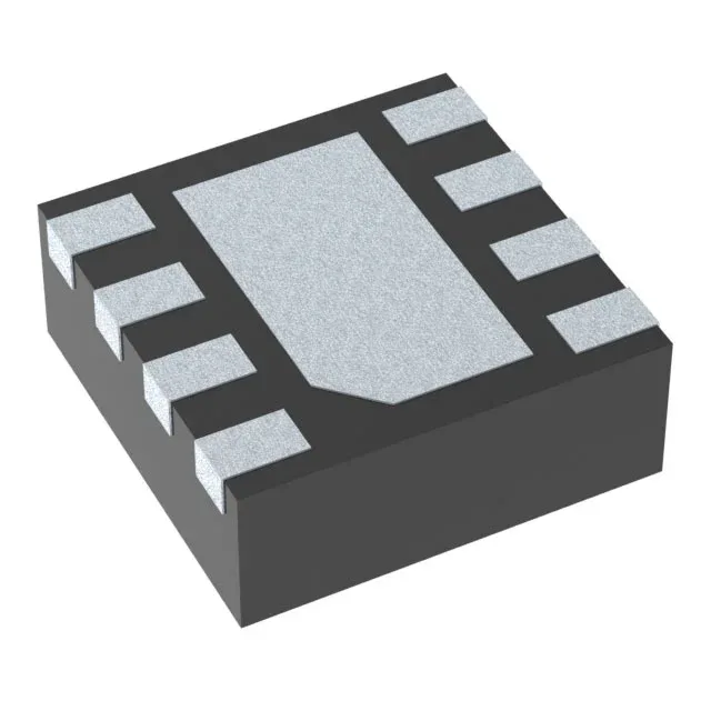
Automotive-grade 3.3 V rail in a 2 mm × 2 mm footprint
The TPS62162QDSGRQ1 is a fixed 3.3 V output, 1 A step-down converter from TI's automotive-qualified DCS-Control™ family. It integrates the synchronous rectifier and compensation, so the BOM stays lean — no external feedback divider, no loop-stability tweaking. The 2.25 MHz switching frequency lets the designer use a small inductor, keeping the total solution footprint tight around the 2 mm × 2 mm package.
What the 1 A and 3.3 V fixed output mean for the BOM
At 1 A continuous output, this part covers the 3.3 V rail for a sensor module, a CAN transceiver, or a low-power MCU in an automotive ECU. The fixed 3.3 V output means one fewer resistor divider on the board — the feedback node is internal, so the output capacitor alone sets the loop response. Input range spans 3 V to 17 V, which covers the nominal automotive battery bus and survives load-dump transients within the abs-max rating.
Package and reflow — the 8-WSON with exposed pad
MSL level is not in the record, but the standard TI WSON is MSL-1 or -2; confirm the reel label before the oven.
TI lists the TPS62162QDSGRQ1 as Active. The base product number TPS62162 spans multiple voltage options in the same package, so the manufacturing line is stable.