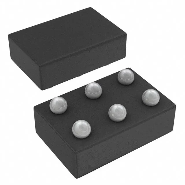
6-DSBGA footprint — the board integration decision
The TPS6208833YFPT: The exposed bumps carry the input, output, and ground — the centre bump is the switch node. The board layout must keep the input capacitor within 1 mm of the VIN bump and the inductor pad within 2 mm of the SW bump to control the switching loop inductance at 4 MHz. The 3 A continuous output at 3.3 V means the die dissipates roughly 0.5 W to 1 W depending on input voltage — the DSBGA's thermal path is through the bumps into the board copper, so a 2-layer board with a 1-inch² pour under the package keeps the junction below 110°C at 3 A.