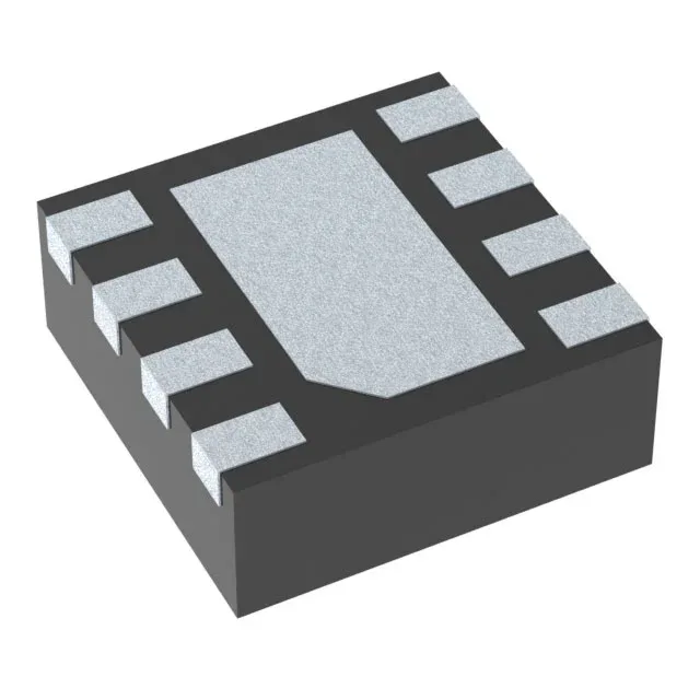
Texas Instruments TPS62080DSGT — Power Management (PMIC / Gate Driver)

TPS62080DSGT Texas Instruments DCS-Control Buck Regulator

MPNTPS62080DSGT
Active

Texas Instruments TPS62080DSGT, DCS-Control™ series, step-down (buck) regulator, adjustable output, 1.2 A output current, 2 MHz switching frequency, 8-WFDFN exposed pad (8-WSON 2×2), surface mount.

$2.0700Ref. price · indicative, final on quote
Packaging8-WFDFN Exposed Pad
RoHSROHS3 Compliant
SeriesDCS-Control™
Independent supplier — new & surplus stockAuthenticity-screened · ESD-safe packingListing updated Aug 2026

Specifications

TPS62080DSGT specifications
ParameterValue
SeriesDCS-Control™
Output typeAdjustable
MountingSurface Mount
Voltage - input2.3V
Voltage - output4V
Voltage - output (Min (Fixed))0.5V
Output current1.2A
Frequency2MHz
I/O channels1
Operating temperature-40°C~85°C(TA)
PackageTape & Reel (TR); Cut Tape (CT)
FunctionStep-Down
TopologyBuck
Case8-WFDFN Exposed Pad
Output configurationPositive
Synchronous rectifierYes

Product details

What this 1.2 A buck regulator delivers in a 2×2 mm package

The TPS62080DSGT is a synchronous step-down converter from Texas Instruments' DCS-Control™ family, delivering up to 1.2 A from a 2.3 V to 6 V input rail.

Sizing the inductor and setting the output voltage

Because the switching frequency is fixed at 2 MHz, the inductor ripple current scales with the input-to-output voltage differential. For a typical 3.3 V to 1.8 V conversion at 1.2 A, a 1.5 µH inductor keeps ripple under 30 % of the load. The 2.3 V minimum input voltage allows operation from a single Li-ion cell (3.0 V to 4.2 V) with margin for battery discharge down to 2.3 V. The 6 V maximum input suits 5 V regulated rails or two-cell alkaline stacks.

No direct second-source exists in the same footprint; the closest functional alternative from TI is the LMR33630APCQRNXRQ1, which offers 3 A output in a larger package with a wider input range, but it is not pin-compatible.

Layout checklist for the 8-WSON exposed pad

The 8-WSON (2×2) package has a 2 mm × 2 mm body with an exposed thermal pad on the bottom. The input capacitor (10 µF ceramic) should sit within 2 mm of the VIN pin; the output capacitor (22 µF ceramic) within 2 mm of the VOUT pin. Because the part is a synchronous buck, the switch node (SW) has fast edges at 2 MHz. Keep the SW trace short and away from the feedback (FB) trace to avoid coupling. The feedback resistor divider should be placed close to the FB pin with the upper resistor connected to VOUT and the lower to GND.

Frequently asked questions

What is the price of TPS62080DSGT in 1000-piece quantities?

Bulk pricing directly impacts BOM cost for volume buyers.

Is TPS62080DSGT in stock at Digi-Key or Mouser?

Availability determines ability to meet production deadlines.

What is the exact pinout and thermal pad footprint of TPS62080DSGT?

Design engineers need precise footprint for PCB layout to ensure proper fit.

What is the output voltage adjust range and maximum load current for TPS62080DSGT?

Engineers must confirm the part meets their voltage and current requirements.

Can TPS62080DSGT be replaced with an equivalent part if unavailable?

Sourcing buyers need drop-in alternatives to avoid redesigns.

What is the lead time and lifecycle status (obsolete? active?) of TPS62080DSGT?

Long lead time or end-of-life can force a last-time buy or redesign.