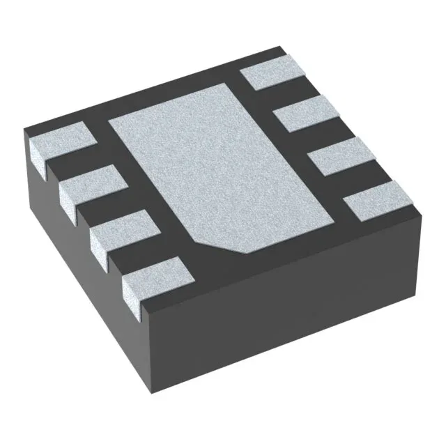
Texas Instruments TPS62067QDSGRQ1 — Power Management (PMIC / Gate Driver)

TPS62067QDSGRQ1 – 2A Automotive Buck Regulator, 3 MHz

MPNTPS62067QDSGRQ1
Active

Texas Instruments TPS62067QDSGRQ1, Automotive AEC-Q100, Step-Down Buck Regulator, Adjustable Output, 2A, 3MHz, 8-WFDFN Exposed Pad (8-WSON 2x2 mm), Active Production

$2.2200Ref. price · indicative, final on quote
Packaging8-WFDFN Exposed Pad
RoHSROHS3 Compliant
SeriesAutomotive, AEC-Q100
Independent supplier — new & surplus stockAuthenticity-screened · ESD-safe packingListing updated Aug 2026

Specifications

TPS62067QDSGRQ1 specifications
ParameterValue
SeriesAutomotive, AEC-Q100
Output typeAdjustable
MountingSurface Mount
Voltage - input2.9V
Voltage - output6V
Voltage - output (Min (Fixed))0.8V
Output current2A
Frequency3MHz
I/O channels1
Operating temperature-40°C~125°C(TJ)
PackageTape & Reel (TR); Cut Tape (CT)
FunctionStep-Down
TopologyBuck
Case8-WFDFN Exposed Pad
Output configurationPositive
Synchronous rectifierYes

Product details

2A at 3 MHz — the switching-frequency trade-off

The TPS62067QDSGRQ1 is a 2A continuous-output, synchronous buck regulator switching at 3 MHz.

Input range and adjustable output

Input voltage spans 2.9 V to 6 V, which covers common automotive battery rails and post-regulated supplies from a wider front-end. The output is adjustable from 0.8 V up to 6 V via an external resistor divider — the 0.8 V reference is the floor for low-voltage core rails. The 3 MHz fixed switching frequency keeps the ripple within the feedback loop bandwidth, so the output stays stable across the full load range without external compensation components.

Package and footprint reality: 8-WSON (2x2 mm)

The 8-WFDFN exposed-pad package (supplier device package 8-WSON 2x2 mm) is the physical constraint. Without that thermal management, the junction temperature rise at 2 A output can exceed the 125°C limit in a 85°C ambient. The 0.50 mm pitch of the WSON demands a controlled solder paste stencil; the pad geometry is standard for this package family, so the footprint is available in most PCB layout libraries.

For a BOM line in an automotive program with a multi-year production horizon, this status means the supply chain is stable — no urgent LTB math needed.

Frequently asked questions

What is the output current of TPS62067QDSGRQ1?

The device is rated for 2 A continuous output. At 3 MHz switching frequency, the inductor and output capacitor can be small, but the 2 A rating is real only when the exposed pad thermal management is adequate — see the package section above.