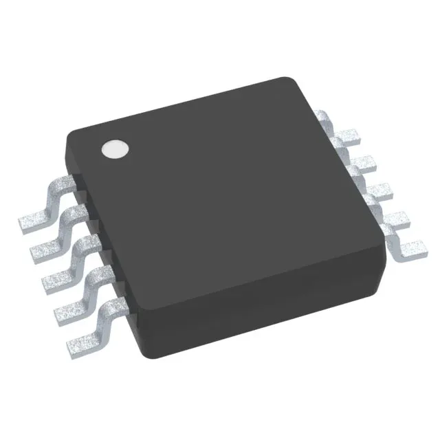
Texas Instruments TPS62051DGSRG4 — Power Management (PMIC / Gate Driver)

TPS62051DGSRG4 Step-Down Regulator, 800 mA, 10-VSSOP

MPNTPS62051DGSRG4
End of Life

Texas Instruments TPS62051DGSRG4, Step-Down Buck Regulator, Adjustable Output, 800 mA, 850 kHz, 10-VSSOP, -40°C to 125°C.

$0.9504Ref. price · indicative, final on quote
Independent supplier — new & surplus stockAuthenticity-screened · ESD-safe packingListing updated Jul 2026

Specifications

TPS62051DGSRG4 specifications
ParameterValue
Output typeAdjustable
MountingSurface Mount
Voltage - input2.7V
Voltage - output6V
Voltage - output (Min (Fixed))0.7V
Output current800mA
Frequency - switching850kHz
I/O channels1
Operating temperature-40°C ~ 125°C (TJ)
PackageTape & Reel (TR)
FunctionStep-Down
TopologyBuck
Case10-TFSOP, 10-MSOP (0.118\", 3.00mm Width)
Output configurationPositive
Synchronous rectifierYes

Product details

The TPS62051DGSRG4 is a 800 mA synchronous buck converter from TI's TPS6205x family, packing a step-down regulator into a 10-VSSOP package. It takes a 2.7 V to 10 V input rail and delivers an adjustable output from 0.7 V up to 6 V — covering everything from a 1.2 V FPGA core to a 5 V sensor supply. The 850 kHz fixed switching frequency keeps the external inductor small — typically a 4.7 µH or 10 µH part — which is the whole point of this regulator: you trade a little efficiency at very light loads for a compact, low-BOM-count power stage. The synchronous rectifier is integrated, so there is no external Schottky diode to place or fail. On a repair bench, when a board with this regulator goes dead, the scorch mark is usually on the input cap or the inductor, not the IC itself — the TPS62051 is a tough part.

Output voltage range and thermal envelope

The output adjusts from a 0.7 V minimum up to 6 V maximum, set by a resistor divider on the FB pin. That 0.7 V floor is low enough to power modern 0.9 V or 1.0 V core rails on DSPs or FPGAs, while the 6 V ceiling handles legacy 5 V logic or analog supplies. The 125°C ceiling is the junction limit, so ambient temperature plus self-heating from the 800 mA load must stay under that number.

No official successor has been designated, which means the base TPS62051 die is the current design-in target.

Frequently asked questions

What is the closest pin-compatible alternative to TPS62051DGSRG4 in this component family?

Within the TPS6205x family, the TPS62050 is a functional sibling sharing the same pinout and package, but it delivers a fixed output voltage rather than the adjustable output of the TPS62051. The TPS62051DGSRG4 is the adjustable-output variant; the TPS62050 is fixed-output. Footprint and pin compatibility are identical, so a board designed for one can accept the other with a resistor-divider change on the FB pin.