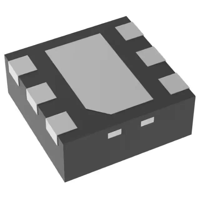
Texas Instruments TPS61291DRVT — Power Management (PMIC / Gate Driver)

TPS61291DRVT Boost Converter – TI, 0.9V-5V Input

MPNTPS61291DRVT
Active

Texas Instruments TPS61291DRVT, a synchronous step-up (boost) DC-DC converter, 0.9 V to 5 V input, programmable output 2.5 V / 3 V / 3.3 V, 700 mA switch, 6-WSON (2x2 mm) package.

$2.0100Ref. price · indicative, final on quote
Packaging6-WDFN Exposed Pad
RoHSROHS3 Compliant
Independent supplier — new & surplus stockAuthenticity-screened · ESD-safe packingListing updated Aug 2026

Specifications

TPS61291DRVT specifications
ParameterValue
Output typeProgrammable
MountingSurface Mount
Voltage - input0.9V
Voltage - output (Min (Fixed))2.5V, 3V, 3.3V
Output current700mA (Switch)
I/O channels1
Operating temperature-40°C~85°C(TA)
PackageTape & Reel (TR); Cut Tape (CT)
FunctionStep-Up
TopologyBoost
Case6-WDFN Exposed Pad
Output configurationPositive
Synchronous rectifierYes

Product details

Low-voltage start-up for single-cell battery rails

The TPS61291DRVT is a synchronous boost converter that starts from an input as low as 0.9 V and delivers a programmable output of 2.5 V, 3 V, or 3.3 V. The 700 mA internal switch handles loads typical for sensor nodes, Bluetooth modules, and small MCU rails without an external FET.

700 mA switch current and synchronous rectification

With a 700 mA switch and integrated synchronous rectifier, the TPS61291DRVT avoids the efficiency penalty of an external Schottky diode. The 0.9 V minimum input means a single alkaline cell at 1.0 V still regulates — useful for battery-powered gear that must run until the cell is nearly flat.

Active production in a compact 6-WSON package

The 6-WSON (2x2 mm) package with exposed pad helps pull heat into the PCB copper.

Industrial temperature range and board fit

No automotive qualification is listed, so keep it out of under-hood designs.

Frequently asked questions

Does TPS61291DRVT require external resistors to set the output voltage?

No. The output is programmable to 2.5 V, 3 V, or 3.3 V via a logic pin — no external feedback divider needed. This saves two resistors and a feedback node on the PCB.