4 A switch in a 1.67 mm square — what it buys you
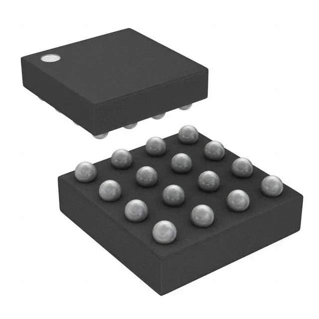
The TPS61282YFFR is a Texas Instruments step-up (boost) converter delivering up to 4 A through its integrated switch in a 16-bump DSBGA package measuring just 1.67 x 1.67 mm. The switching frequency is fixed at 2.3 MHz, which keeps the inductor small — typically a 1 µH to 2.2 µH shielded type — and pushes the output ripple above the 20 kHz audio band. The output is programmable via external feedback resistors, with a minimum fixed output of 2.85 V and a maximum of 4.4 V, making it a fit for powering a 3.3 V or 3.8 V rail from a single Li-ion cell or 2.3 V to 4.85 V input bus. The single positive output is configured for step-up only; this is not a buck-boost topology, so the input must stay below the output voltage target.
Obsolete — plan the last-time buy or qualify the alternate now
That means TI has stopped production; no further factory orders can be placed. Any remaining stock in the independent distribution channel is what exists — no replenishment. The base product number is TPS61282, and the YFFR suffix denotes the 16-DSBGA package and tape-and-reel shipping medium. If you are looking for a pin-compatible drop-in, there is no confirmed second-source or direct replacement from TI at this writing. A functional replacement — same boost topology, similar switch current and frequency — will require a PCB layout change because the DSBGA footprint is unique to this package variant.
DSBGA layout and rework realities
The 16-DSBGA package (1.67 x 1.67 mm) uses 0.4 mm pitch solder balls arranged in a 4 x 4 array. That pitch is fine enough that a standard two-layer board with 0.5 mm vias can fan out the inner rows, but the trace width between balls is limited to about 0.15 mm — a 4-layer stack-up with microvias is cleaner for high-current paths. The centre balls carry the switch node and ground; the thermal dissipation relies on the PCB copper area, not an exposed pad. For rework, a hot-air profile with a bottom preheat at 100 °C and a top nozzle at 260 °C peak is typical; the DSBGA is moisture-sensitive, so a bake at 125 °C for 24 hours is needed if the floor life has been exceeded. The input voltage range is 2.3 V to 4.85 V, which covers a single Li-ion cell (3.0 V to 4.2 V nominal) and two alkaline cells in series. The output is programmable up to 4.4 V, so this part cannot generate a 5 V rail. The 4 A switch current is the peak inductor current limit, not the continuous output current — the actual output current depends on the input-to-output voltage ratio and efficiency. At a 3.3 V output from a 3.0 V input, expect about 2.5 A continuous output before hitting the current limit.