Active production — sourcing the TPS61282DYFFT
Boost topology with 4 A switch and 2.3 MHz switching
This is a single-output step-up (boost) regulator with a 4 A switch current rating — that 4 A is the peak switch limit, not the output current; the achievable output current depends on input voltage, output voltage, and inductor ripple. The 2.3 MHz switching frequency lets you use a smaller inductor (typically 1 µH to 2.2 µH) than a 1 MHz part, shrinking the PCB footprint.
Temperature range and package — reflow and placement
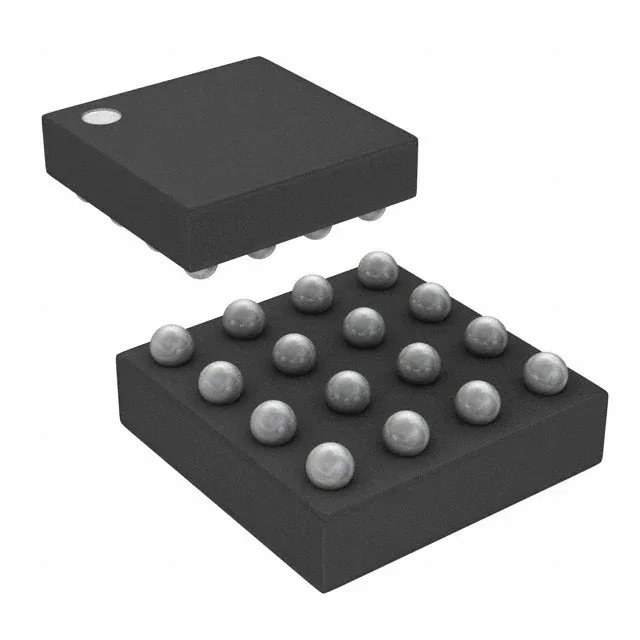
The 16-DSBGA package (1.67 mm × 1.67 mm) is a wafer-level chip-scale package: no leads, no exposed pad. The solder balls are on the bottom; the board footprint must match the 0.4 mm pitch ball map exactly. The package sits flat with no tombstoning risk if the stencil aperture is sized per TI's application note for DSBGA.
Input voltage range and output voltage flexibility
Input voltage range is 2.3 V to 4.85 V — covers single-cell Li-ion (3.0 V to 4.2 V) and two-cell alkaline (2.4 V to 3.0 V). The output can be set from a minimum of 3.15 V up to 4.4 V, making it suitable for powering a 3.3 V rail with headroom or a 3.6 V to 4.2 V LED backlight string.