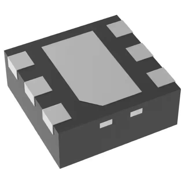
Texas Instruments TPS61261DRVR — Power Management (PMIC / Gate Driver)

TPS61261DRVR – Texas Instruments Boost Converter

MPNTPS61261DRVR
Active

Texas Instruments TPS61261DRVR, a step-up boost regulator with fixed 3.3V output, 100mA current capability, 2.5MHz switching frequency, 0.8V to 4V input range, in a 6-WSON (2x2 mm) package.

$1.2800Ref. price · indicative, final on quote
Packaging6-WDFN Exposed Pad
RoHSROHS3 Compliant
Independent supplier — new & surplus stockAuthenticity-screened · ESD-safe packingListing updated Aug 2026

Specifications

TPS61261DRVR specifications
ParameterValue
Output typeFixed
MountingSurface Mount
Voltage - input0.8V
Voltage - output (Min (Fixed))3.3V
Output current100mA
Frequency2.5MHz
I/O channels1
Operating temperature-40°C~85°C(TA)
PackageTape & Reel (TR); Cut Tape (CT)
FunctionStep-Up
TopologyBoost
Case6-WDFN Exposed Pad
Output configurationPositive
Synchronous rectifierYes

Product details

What this boost regulator does for a single-cell rail

The TPS61261DRVR is a fixed 3.3V output boost converter from Texas Instruments, designed to step up a low-voltage input as low as 0.8V to a regulated 3.3V rail at up to 100mA. Its 2.5MHz switching frequency keeps the inductor and output capacitor small — a 1µH inductor and 4.7µF ceramic cap typically fit the bill, which matters when board space is tight. The synchronous rectifier improves efficiency at light loads compared to a diode-based boost, so a battery-powered design sees longer run time between charges.

Minimum input of 0.8V means this part can pull a single alkaline cell down to nearly dead and still hold the 3.3V output — useful for a remote sensor or a Bluetooth beacon running on one AA. Maximum input of 4V sets the ceiling: you cannot feed it from a 5V rail or a two-cell Li-ion stack without a pre-regulator. Output is fixed at 3.3V — no feedback resistor network needed, which saves two components and one potential noise injection point on the layout.

Package and thermal — the 6-WSON footprint

Without that thermal via cluster, the 100mA output derates above 70°C ambient. The 2x2 mm footprint is small enough for wearable or IoT modules, but the 0.5 mm pitch on the WSON pads demands a soldermask-defined pad and a stencil aperture that matches the datasheet recommendation.

ROHS3 compliant.

Frequently asked questions

What are the specifications of TPS61261DRVR?

Designers need exact specs for fit and performance before selecting the part.

What is the price of TPS61261DRVR in quantity?

Buyers compare pricing for BOM cost estimation and sourcing decisions.

Where can I buy TPS61261DRVR with stock?

Availability directly impacts production schedule; engineers and buyers need source leads.

Is there a replacement or equivalent for TPS61261DRVR?

If the part is out of stock or obsolete (though currently active), cross-references enable design continuity.

What is the input voltage range of TPS61261DRVR?

Critical for validating if the part works with the given power source in the design.

Is TPS61261DRVR still in production or EOL?

Lifecycle status determines long-term availability and risk of redesign for buying and maintenance teams.