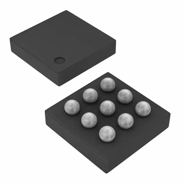
3.9A switch, 9-DSBGA — what the boost delivers
The Texas Instruments TPS61258YFFR is a fixed-output step-up (boost) converter built around a 3.9A integrated switch, switching at 3.5 MHz. The 2.65 V to 4.35 V input range and fixed 4.5 V output target single-cell Li-ion or 3.3 V rail applications that need a regulated 4.5 V bus — USB OTG, sensor bias, or small motor pre-drive supplies. The 9-DSBGA package (0.8 mm × 0.8 mm nominal) and 3.5 MHz switching let the designer shrink the inductor to a 1.0 mm × 0.5 mm footprint and use a 4.7 µH or 2.2 µH part, keeping the total solution area under 10 mm².
3.5 MHz — inductor and capacitor selection
The 3.5 MHz switching frequency pulls the inductor value down to the 1 µH to 4.7 µH range, which fits a 1008 or 0805 footprint. The trade-off is switching loss: at light loads the quiescent current matters more than the core loss, so the efficiency curve at 1 mA to 10 mA output is worth checking against the battery life target. Synchronous rectification keeps the rectifier drop below 100 mV at moderate loads, which helps hold efficiency above 85% across the 50 mA to 500 mA output range typical for a 4.5 V rail.
DSBGA footprint — layout constraints
The 9-DSBGA (9-bump wafer-level chip-scale package) has a 0.5 mm bump pitch. The board requires a 4-layer stack-up with microvias or via-in-pad to route the input, output, and switch node traces without choking the 3.9 A peak current. The thermal pad on the DSBGA is the backside of the die — solder the bumps and rely on the copper pours on layer 2 for heat spreading.