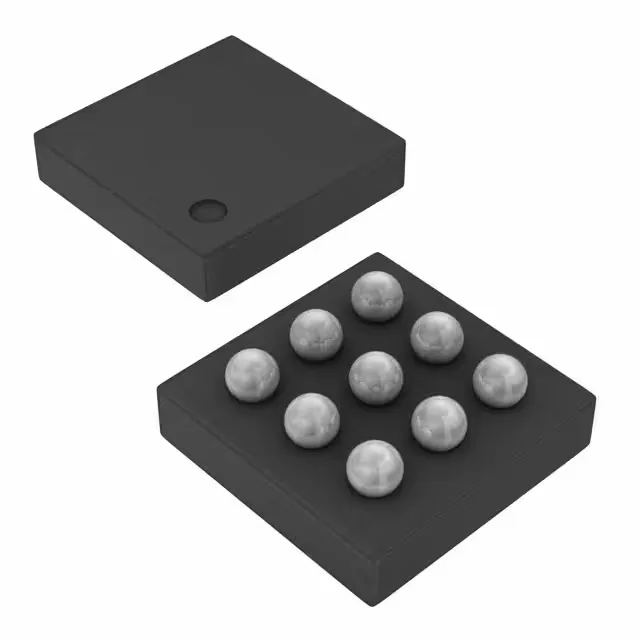
Texas Instruments TPS61254YFFT — Power Management (PMIC / Gate Driver)

TPS61254YFFT Boost Converter 4.5V Fixed 2.4A 9-DSBGA

MPNTPS61254YFFT
Active

Texas Instruments TPS61254YFFT, step-up boost regulator, fixed 4.5V output, 2.4A switch current, 3.5MHz switching frequency, 9-bump DSBGA package, -40°C to 85°C operation.

$1.5700Ref. price · indicative, final on quote
Packaging9-UFBGA, DSBGA
RoHSROHS3 Compliant
Independent supplier — new & surplus stockAuthenticity-screened · ESD-safe packingListing updated Aug 2026

Specifications

TPS61254YFFT specifications
ParameterValue
Output typeFixed
MountingSurface Mount
Voltage - input4.35V
Voltage - output (Min (Fixed))4.5V
Output current2.4A (Switch)
Frequency3.5MHz
I/O channels1
Operating temperature-40°C~85°C(TA)
PackageTape & Reel (TR); Cut Tape (CT)
FunctionStep-Up
TopologyBoost
Case9-UFBGA, DSBGA
Output configurationPositive
Synchronous rectifierYes

Product details

Fixed 4.5V boost with 2.4A switch in a 9-bump DSBGA

The TPS61254YFFT is a fixed-output step-up (boost) converter from Texas Instruments that delivers a regulated 4.5V rail from a 2.5V to 4.35V input source. Its internal switch is rated for 2.4A, which sets the practical load ceiling — at 4.5V out, that switch current translates to roughly 1.5A to 1.8A output depending on efficiency and input voltage. The 3.5MHz switching frequency lets you use a small inductor (typically 1 µH to 2.2 µH) and small ceramic caps, keeping the total solution area tight. The output is fixed at 4.5V, which is a common rail for USB On-The-Go, Li-ion boost to 5V-ish logic, or powering a small sensor node from a single-cell battery.

Package and thermal reality for a 9-DSBGA

The 9-bump DSBGA (0.4mm pitch typical) is a wafer-level package with no mould compound — the die is the package. That means the board footprint is tiny (under 2 mm²), but the thermal path is through the solder bumps to the PCB copper. For a boost converter switching 2.4A, the copper area under the device and the number of via drops to the inner layers directly set the junction temperature. At 85°C ambient and full load, the thermal budget is tight; a 2-layer board with minimal copper may force derating.

ROHS3 compliant.

Frequently asked questions

What is the output voltage of TPS61254YFFT?

Designers need to confirm the fixed output matches their rail requirement before circuit integration.

Is TPS61254YFFT obsolete or active?

Buyers and brokers must verify lifecycle status to avoid supply chain disruptions or end-of-life risks.

Where can I buy TPS61254YFFT in stock?

Sourcing buyers need immediate availability to fill BOM lines without production delays.

What is the price of TPS61254YFFT?

Procurement teams compare pricing across distributors to control project costs.

What is the pinout of TPS61254YFFT?

Design engineers require PCB layout compatibility and pin function verification.

Is TPS61254YFFT a direct replacement for TPS61252?

Maintenance techs and buyers need to confirm drop-in suitability for existing designs or repairs.