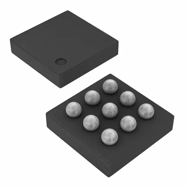
The TPS61253AYFFT is a fixed 5V output synchronous boost converter from Texas Instruments, switching at 3.5 MHz and rated for a 4.6A internal switch current. The high switching frequency shrinks the inductor and output capacitor to 1 µH / 10 µF class values — the trade-off is higher switching losses at light load, but the synchronous rectifier (internal low-side FET replacing the Schottky diode) recovers about 0.35V of forward drop, keeping efficiency above 90% across most of the load range. Input range is 2.3V to 5.5V, so it boots from a single-cell Li-ion at nominal 3.6V or from a 3.3V regulated rail. The 2.3V minimum means it won't start below that — a depleted Li-ion at 2.5V is fine, but cold-cranking a 5V rail from a 1.8V source requires a different part (the TPS6125x family with lower min Vin). Output is fixed at 5V — no external divider, no adjustment. If the load needs 3.3V or an adjustable output, step to the TPS61253A adjustable variant.
9-DSBGA: wafer-level chip-scale footprint
The package is a 9-bump DSBGA (wafer-level chip-scale) on 0.5 mm pitch. There are no leads — the bumps are the terminals. PCB fan-out requires micro-vias or very fine trace/space (0.10 mm / 0.10 mm minimum) to route the 5V output, input, and ground bumps to the inner layers. A two-layer board is possible if the ground bump is stitched with multiple vias; a four-layer stack-up with a dedicated ground plane below the converter is the safer call for thermal and EMI. The 3.5 MHz switching frequency places the fundamental switching harmonic around 7 MHz and the second at 10.5 MHz — keep the input capacitor (10 µF X5R 6.3V or 10V) within 2 mm of the VIN bump, and the output capacitor (22 µF X5R 6.3V) within 2 mm of the VOUT bump. The inductor's self-resonant frequency should be above 20 MHz; a 1 µH shielded inductor rated for 5 A saturation handles the 4.6A switch peak.
Active lifecycle, no automotive qualification
It is not AEC-Q100 qualified, so it is not suited for automotive-grade applications (powertrain, chassis, ADAS) without additional qualification work. The part is procured per BOM quantity.