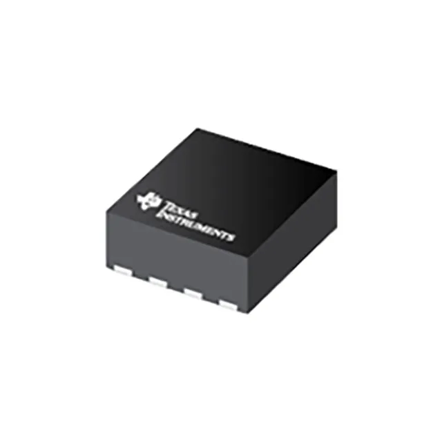
Boost regulator with a 6A internal switch — what that means for your rail
The TPS61230ARNSR is a synchronous step-up (boost) converter from Texas Instruments that integrates a 6A switch, making it suited for applications that need to pull a 2.5V to 4.5V input rail up to an adjustable output as high as 5.5V. The 6A switch current rating is the headline figure — it tells you the peak current the internal FET can handle each switching cycle, which directly sets the maximum output power you can deliver at a given input voltage and duty cycle. Synchronous rectification (the internal low-side and high-side FETs) improves efficiency across the load range compared to a diode-based boost, but the hard-switching edges at 1.15 MHz produce a noise spectrum that matters if this rail feeds a sensitive analog or RF load.
Input range, output adjustability, and the 1.15 MHz switching frequency
The input range runs from 2.5V minimum up to 4.5V maximum — typical sources are a single Li-ion cell (3.0-4.2V) or a 3.3V regulated rail. The output is adjustable from a 2.5V floor up to 5.5V via an external resistor divider, so the same part can serve a 3.3V, 5V, or in-between rail. A single-output, positive-configuration boost with adjustable feedback — the FB pin compares the divided output against a 0.6V internal reference. The compensation is internal, so the external BOM is just the inductor, input/output caps, and feedback resistors.
Package, temperature grade, and board integration
Housed in a 7-VFQFN with supplier device package designation 7-VQFN-HR (2x2 mm) — a 2 mm × 2 mm body with an exposed thermal pad underneath. Rated for junction temperature from -40°C to 125°C, covering industrial ambient environments and the upper end of automotive cabin-temperature applications. The surface-mount package is compatible with standard reflow profiles. ROHS3 compliant per the lifecycle record — no exemptions that would block EU-market shipments. The base product number is TPS61230, and the full suffix ARNSR encodes the reel-and-tape packaging option.
No official second-source or pin-compatible cross-reference is recorded for this order code. If a BOM hedge is needed, the parametric search within the TPS61230 family (same base number, different package/suffix variants) is the starting point.