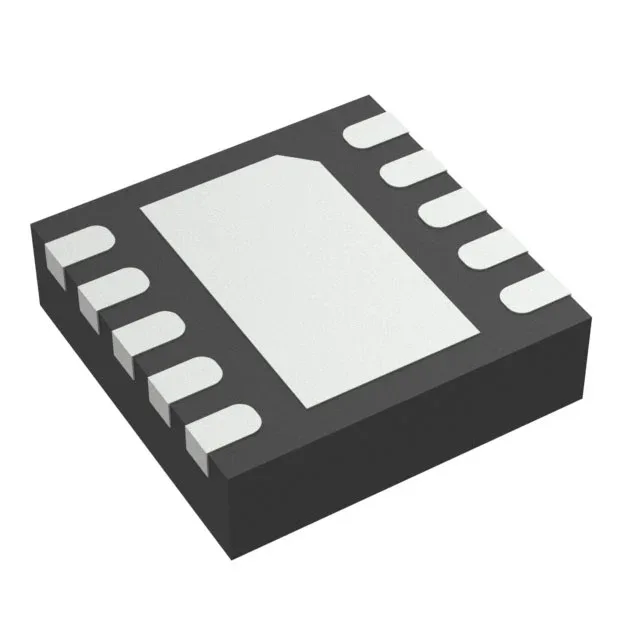
Texas Instruments TPS61200DRCTG4 — DC-DC Power Modules

TPS61200DRCTG4 Boost Converter IC, 0.3 V to 5.5 V Input

MPNTPS61200DRCTG4
End of Life

Texas Instruments TPS61200DRCTG4, Step-Up Boost Converter, 1.2 A Switch, 0.3 V to 5.5 V Input, Adjustable Output, 1.25-1.65 MHz, Synchronous Rectification, 10-VSON (3x3) Exposed Pad, -40 to 85 °C.

$0.9900Ref. price · indicative, final on quote
Independent supplier — new & surplus stockAuthenticity-screened · ESD-safe packingListing updated Jul 2026

Specifications

TPS61200DRCTG4 specifications
ParameterValue
Output typeAdjustable
MountingSurface Mount
Voltage - input5.5V
Voltage - output5.5V
Voltage - output (Min (Fixed))1.8V
Output current1.2A (Switch)
Frequency - switching1.25MHz ~ 1.65MHz
I/O channels1
Operating temperature-40°C~85°C(TA)
PackageTape & Reel (TR)
FunctionStep-Up
TopologyBoost
Case10-VFDFN Exposed Pad
Output configurationPositive
Synchronous rectifierYes

Product details

Boost converter that starts below a dead battery

The Texas Instruments TPS61200DRCTG4 is a synchronous step-up (boost) converter with a minimum input voltage of 0.3 V — low enough to extract usable energy from a single alkaline cell that has dropped below its nominal 1.5 V endpoint, or from a Li-ion cell deep into its discharge curve.

0.3 V minimum input — the so-what for battery-powered BOMs

Most boost converters cut out at 0.8 V or higher. The TPS61200's 0.3 V minimum input means it can start and regulate from a single NiMH, alkaline, or LiFePO4 cell that is nearly fully discharged. For a design targeting a 3.3 V rail from one cell, this extends usable battery life well past the point where a conventional boost would drop out. The trade-off is the input current at low Vin — at 0.3 V in and 3.3 V out at 100 mA, the switch current approaches the 1.2 A limit, so output power is capped at roughly 300 mW at the lowest input. The switching frequency runs between 1.25 MHz and 1.65 MHz, which keeps the inductor small — a 2.2 µH to 4.7 µH shielded ferrite is typical.

Package and thermal: 10-VSON with exposed pad

The TPS61200DRCTG4 is supplied in a 10-VFDFN exposed-pad package, also designated as 10-VSON (3x3 mm).

The base product number is TPS61200, and the DRCTG4 suffix denotes the Tape & Reel (TR) shipping form in the 10-VSON package.

Frequently asked questions

Can TPS61200DRCTG4 be used for a 5 V output application?

Yes. The output is adjustable with a minimum/fixed voltage of 1.8 V and a maximum of 5.5 V. A standard resistor divider from the output to the FB pin sets the regulation point. For a 5 V rail, the input must stay above the minimum 0.3 V and the load current must stay within the power budget set by the 1.2 A switch current limit — at 5 V out from a 3 V input, the maximum output current is roughly 600 mA before the switch hits its limit.

What is the maximum output current of TPS61200?

The switch current limit is 1.2 A. The actual maximum output current depends on the input voltage, output voltage, and efficiency — at a 3.3 V output from a 1.5 V input, expect roughly 400 mA continuous before the switch cycle-by-cycle limit engages.

Is TPS61200DRCTG4 RoHS compliant?

For a formal compliance certificate, request it with your RFQ.