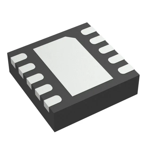
Texas Instruments TPS61200DRCRG4 — DC-DC Power Modules

TPS61200DRCRG4 Boost Converter, 0.3V-5.5V Input, 1.2A Switch

MPNTPS61200DRCRG4
End of Life

Texas Instruments TPS61200DRCRG4, step-up boost converter, 0.3 V to 5.5 V input, 1.8 V to 5.5 V adjustable output, 1.2 A switch current, synchronous rectification, 1.25 MHz to 1.65 MHz switching frequency, 10-VSON (3x3 mm) package, -40°C to 85°C operating temperature.

$0.9900Ref. price · indicative, final on quote
Independent supplier — new & surplus stockAuthenticity-screened · ESD-safe packingListing updated Jul 2026

Specifications

TPS61200DRCRG4 specifications
ParameterValue
Output typeAdjustable
MountingSurface Mount
Voltage - input5.5V
Voltage - output5.5V
Voltage - output (Min (Fixed))1.8V
Output current1.2A (Switch)
Frequency - switching1.25MHz ~ 1.65MHz
I/O channels1
Operating temperature-40°C~85°C(TA)
PackageTape & Reel (TR)
FunctionStep-Up
TopologyBoost
Case10-VFDFN Exposed Pad
Output configurationPositive
Synchronous rectifierYes

Product details

0.3 V minimum input — the battery-extraction boost

The TPS61200DRCRG4 is a synchronous step-up (boost) converter from Texas Instruments that starts up and regulates from an input voltage as low as 0.3 V. The 1.2 A switch current limit sets the output power ceiling — at 3.3 V out from a 1.5 V input, budget around 1.5 W continuous before the switch hits its limit.

Synchronous rectification — one less Schottky on the BOM

This part integrates a synchronous rectifier, so there is no external Schottky diode in the boost path. That saves a component, shrinks the layout, and improves efficiency at light loads compared to a non-synchronous boost with a discrete diode. The switching frequency runs between 1.25 MHz and 1.65 MHz, which keeps the inductor small — typically a 2.2 µH to 4.7 µH shielded part in the 3x3 mm footprint.

10-VSON exposed pad — thermal design is not optional

The package is a 10-VFDFN with an exposed pad, also called 10-VSON (3x3 mm). Surface-mount assembly with standard lead-free reflow — the exposed pad does not require a special profile, but the solder stencil aperture under the pad should be segmented to avoid voiding.

Frequently asked questions

What is the datasheet for TPS61200DRCRG4?

Engineers need full specifications, pinout, and application circuits to validate fit in their design.

What is the price of TPS61200DRCRG4?

Buyers compare costs across distributors to optimize BOM spend.

Is TPS61200DRCRG4 in stock?

Availability directly impacts procurement lead times and production schedules.

What is the equivalent of TPS61200DRCRG4?

Sourcing buyers and brokers need drop-in replacements when the exact part is unavailable or costly.

Where can I buy TPS61200DRCRG4?

Transactional buyers need authorized distributor links to complete the purchase quickly.

What is the pinout of TPS61200DRCRG4?

Maintenance techs and design engineers require correct pin mapping for board integration or replacement.