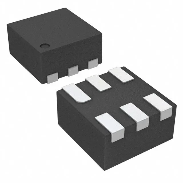
Texas Instruments TPS610986DSET — Power Management (PMIC / Gate Driver)

TI TPS610986DSET boost+LDO, dual 3.3V output, 350mA/200mA

MPNTPS610986DSET
Active

Texas Instruments TPS610986DSET, step-up (boost) synchronous converter with integrated LDO, dual 3.3V outputs (350mA / 200mA), 0.7V to 4.5V input, -40 to 85°C, 6-WSON (1.5x1.5 mm).

$1.8000Ref. price · indicative, final on quote
Independent supplier — new & surplus stockAuthenticity-screened · ESD-safe packingListing updated Jul 2026

Specifications

TPS610986DSET specifications
ParameterValue
MountingSurface Mount
Supply voltage0.7V ~ 4.5V
Voltage/Current - output 13.3V, 350mA
Voltage/Current - output 23.3V, 200mA
I/O channels2
Operating temperature-40°C~85°C(TA)
PackageTape & Reel (TR); Cut Tape (CT)
TopologyStep-Up (Boost) Synchronous (1), Linear (LDO) (1)
W (Sequencer)No
W (LED driver)No
W (Supervisor)No
Case6-WFDFN

Product details

Dual 3.3 V rails from a single boost plus LDO

The TPS610986DSET from Texas Instruments combines a synchronous step-up (boost) converter with an integrated linear regulator (LDO) to deliver two regulated 3.3 V outputs from a single input supply. Output 1 is rated for 350 mA, output 2 for 200 mA, both at 3.3 V. The input range spans 0.7 V to 4.5 V, which lets it start from a single alkaline cell or a Li-ion battery and continue operating as the cell voltage drops.

0.7 V minimum input — cold-start from a near-dead cell

The 0.7 V minimum supply voltage is the headline spec for battery-powered designs. It means the boost converter can start up and regulate from a single alkaline cell that has discharged to 0.7 V, or from a Li-ion cell well below its typical 3.0 V cutoff. The synchronous topology keeps conversion efficiency high — no external Schottky diode needed — which matters when every milliwatt extends run time.

6-WSON 1.5x1.5 mm — board-area trade-off

The 6-WSON package measures 1.5 x 1.5 mm, which saves board space but demands careful layout. The 0.5 mm pitch limits breakout to two-layer boards; a four-layer stack with a dedicated ground plane under the pad is the safer route for 350 mA continuous output.

Frequently asked questions

Can TPS610986DSET be used in a 3.3 V output design?

Yes, both outputs are fixed at 3.3 V. Output 1 delivers up to 350 mA, output 2 up to 200 mA. The input can be as low as 0.7 V, so it works with a single-cell battery or a 3.3 V rail that needs a clean secondary output.

What package is TPS610986DSET?

It is supplied in a 6-WFDFN package, specifically a 6-WSON (1.5 x 1.5 mm) with an exposed thermal pad. The supplier device package code is 6-WSON (1.5x1.5).