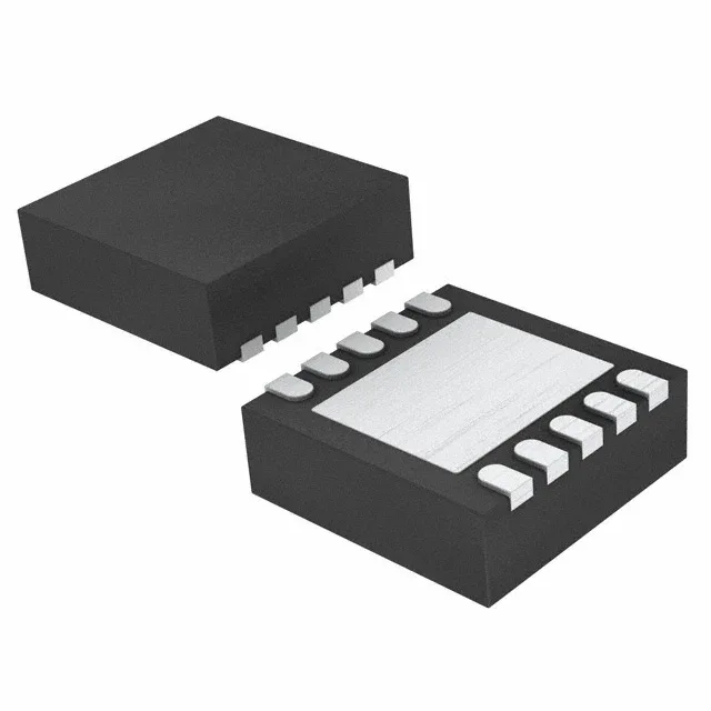
Texas Instruments TPS61093DSKR — DC-DC Power Modules

Texas Instruments TPS61093DSKR Step-Up Boost Converter

MPNTPS61093DSKR
Active

Texas Instruments TPS61093DSKR step-up (boost) DC-DC converter, adjustable output, 1.6 V to 6 V input range, 900 mA (switch) output current, 1.2 MHz switching frequency, -40°C to 85°C, 10-WFDFN exposed-pad package, surface mount.

$2.3700Ref. price · indicative, final on quote
Independent supplier — new & surplus stockAuthenticity-screened · ESD-safe packingListing updated Jul 2026

Specifications

TPS61093DSKR specifications
ParameterValue
Output typeAdjustable
MountingSurface Mount
Voltage - input1.6V
Voltage - output17V
Voltage - output (Min (Fixed))1.6V
Output current900mA (Switch)
Frequency - switching1.2MHz
I/O channels1
Operating temperature-40°C~85°C(TA)
PackageTape & Reel (TR); Cut Tape (CT)
FunctionStep-Up
TopologyBoost
Case10-WFDFN Exposed Pad
Output configurationPositive
Synchronous rectifierNo

Product details

Boost converter with a 900 mA switch in a 10-WFDFN package

The Texas Instruments TPS61093DSKR is a step-up (boost) DC-DC converter with a 900 mA integrated switch, designed to generate an adjustable output up to 17 V from a low-voltage input source as low as 1.6 V. Switching at a fixed 1.2 MHz, it uses a small inductor and ceramic capacitors to keep the solution footprint compact — a common choice for space-constrained portable or battery-backed rails.

Input voltage range and output headroom

The input range spans 1.6 V to 6 V, so a single Li-Ion cell (3.0 V to 4.2 V), two or three alkaline cells, or a regulated 3.3 V / 5 V rail all fit within the operating envelope. With the output adjustable from 1.6 V up to 17 V, this converter can generate 12 V bias rails, 5 V from a lower battery voltage, or drive a string of white LEDs — the 17 V ceiling gives enough headroom for a 3- or 4-series LED chain.

Switching frequency and external component sizing

The 1.2 MHz switching frequency places the fundamental ripple in the low-MHz band, allowing the use of small-value inductors (typically 4.7 µH to 10 µH) and ceramic output capacitors that keep the total BOM area small. Because the part does not use synchronous rectification (external Schottky diode required), the rectifier forward drop adds to the conduction loss — a 0.4 V to 0.5 V Schottky works well at this voltage and current level.

The small footprint (2.5 mm x 2.5 mm) suits portable and space-limited designs, but the pad clearance and via placement under the package need care during layout.

Active lifecycle — no last-time-buy risk

It can be specified for new production builds without a last-time-buy clock, and the base product number TPS61093 remains in the TI portfolio. For dual-sourcing or supply-resilience planning, there is no official second-source pin-compatible alternate from another manufacturer listed on this record.

Frequently asked questions

Is TPS61093DSKR obsolete or active?

It can be specified for new production without a last-time-buy risk.

What is the output current capability of TPS61093DSKR?

The internal switch is rated for 900 mA peak current. The actual continuous output current depends on the input-to-output voltage ratio and the inductor selection — at moderate step-up ratios (e.g., 3.3 V to 5 V) you can expect several hundred mA to the load.

Does TPS61093DSKR require external compensation?

No, the TPS61093DSKR is internally compensated. The only external components needed are the inductor, input/output capacitors, feedback resistor divider, and a Schottky rectifier diode.

How to set the output voltage on TPS61093DSKR?

The output is adjustable via an external resistor divider from the output to the FB pin. The internal reference is 1.6 V (the minimum output voltage); the divider ratio sets Vout = 1.6 V × (1 + R1/R2).