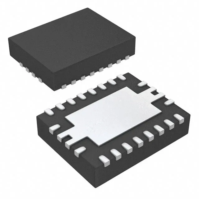
10 A boost in a 3.5 mm × 4.5 mm footprint
The TPS61088RHLR: That current rating is unusually high for a boost IC in a QFN package this size — it forces the designer to pay close attention to the power-stage layout and the thermal pad connection to the ground plane. The synchronous rectifier is built in, which eliminates the external Schottky diode and improves efficiency at heavy loads.
Adjustable output and thermal envelope
Output voltage is adjustable from a 4.5 V minimum up to 12.6 V maximum. The 10 A peak current limit sets the practical output current. The 20-VQFN package with exposed pad (3.5 mm × 4.5 mm) requires a solid thermal via pattern under the pad.
It is supplied in tape-and-reel or cut-tape formats.