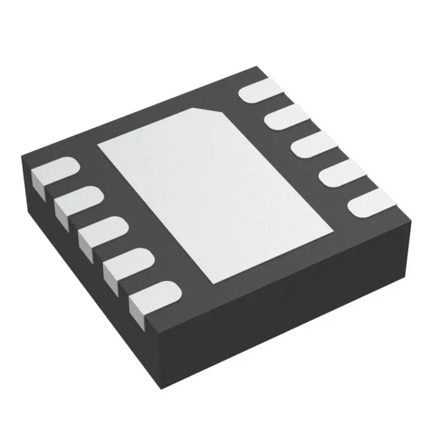
Boost converter for battery-powered rails
The TPS61087DRCT is a step-up (boost) converter from Texas Instruments, designed to generate an adjustable output voltage from 3V up to 18.5V from a 2.5V to 6V input rail. It uses an external Schottky diode (not synchronous rectification), so the efficiency peaks when the output voltage is several times the input, typical in battery-powered displays, white-LED backlights, and portable audio supplies.
Switch current and frequency flexibility
At a typical 5V input and 12V output, that switch current supports roughly 10–12W output, derated for inductor ripple and temperature. The device offers two switching frequency options: 650 kHz and 1.2 MHz, selected via a resistor. The lower frequency favours higher efficiency (less switching loss), while the higher frequency shrinks inductor and capacitor size at the cost of slightly lower efficiency and tighter layout for EMI control.
Thermal and package considerations
The 10-VFDFN exposed pad (10-VSON 3x3 mm) package relies on the PCB copper area attached to the pad for heat dissipation. For higher ambient or higher output power, the PCB layout must include adequate thermal vias and a solid copper pour under the pad to keep the switch junction within its limits.
It is ROHS3 compliant, with no announced end-of-life or PCN at this writing.