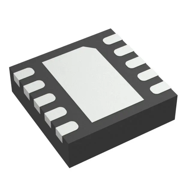
Boost converter with a 3.2 A switch — sizing the power stage
The Texas Instruments TPS61087DRCRG4 is a current-mode step-up (boost) converter with a single integrated 3.2 A switch, adjustable output up to 18.5 V, and a choice of 650 kHz or 1.2 MHz switching frequency. It takes an input from 2.5 V to 6 V and delivers a positive output rail — typical applications include 5 V to 12 V conversion for LCD bias, USB power, and portable equipment where the input comes from a single-cell Li-Ion or multi-cell alkaline stack.
The 3.2 A switch current rating is the peak current the internal NMOS can handle cycle-by-cycle. For a typical 5 V to 12 V boost at 85% efficiency, that works out to about 10 W output — enough to drive a string of LEDs, a small LCD panel, or a sensor module. The actual output current you can pull depends on the input voltage, output voltage, and inductor ripple; at higher step-up ratios the switch current limit becomes the binding constraint, not the output voltage. Because the part lacks synchronous rectification (it uses an external Schottky diode), the efficiency peaks in the 85–90% range at moderate loads. The diode forward drop adds a few percent loss at high output current, but the simplicity keeps the BOM count low.
650 kHz or 1.2 MHz — picking the switching frequency
The TPS61087DRCRG4 lets you select between 650 kHz and 1.2 MHz via a single resistor on the FREQ pin. At 1.2 MHz the inductor can be smaller (2.2 µH to 4.7 µH range), which shrinks the board footprint — useful for space-constrained portable designs. At 650 kHz the switching losses drop and the efficiency ticks up a couple of points, at the cost of a larger inductor (6.8 µH to 10 µH). The 1.2 MHz setting also pushes the fundamental switching harmonic above the AM radio band, which helps in noise-sensitive RF applications.
Package and thermal: 10-VSON with exposed pad
Without that, the junction temperature rises quickly at 3.2 A switching current, especially at high ambient temperatures. The part is not rated for under-hood or engine-bay temperatures (125°C+), so keep that in mind if the end equipment sees sustained heat soak.