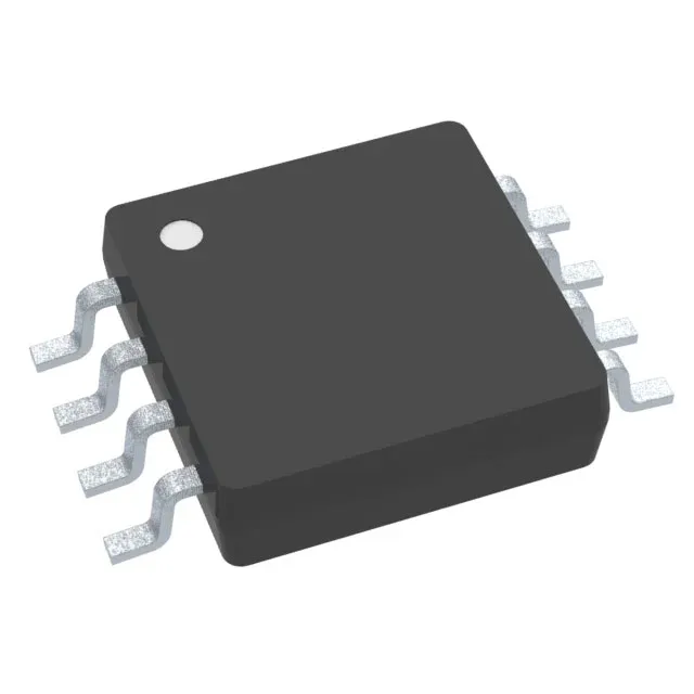
Boost converter with a 2A switch and dual-frequency timing
The TPS61085DGKT is a Texas Instruments step-up (boost) DC-DC converter built around a 2A integrated switch. It accepts an input from 2.3V up to 6V and delivers an adjustable output up to 18.5V — a range that suits single-cell Li-Ion, 3.3V, or 5V rails feeding higher-voltage loads like OLED bias, CCD sensor supplies, or USB-C power-bank rails. The converter operates at a selectable switching frequency of 650 kHz or 1.2 MHz, letting the designer trade inductor size against switching losses and EMI. The lower frequency favours higher efficiency at moderate loads; the higher frequency shrinks the inductor footprint for space-constrained designs.
Selecting the switching frequency for the BOM
At 650 kHz the inductor ripple current is lower, so a standard 10 µH to 22 µH shielded inductor works with acceptable core loss. At 1.2 MHz the inductor drops to 4.7 µH to 10 µH, saving board area but increasing the AC loss in the switch and the inductor core. The pin-strapped frequency selection (a single resistor to GND or VIN) is set at the board layout stage and cannot be changed in-circuit. The 2A switch current rating is the peak current through the internal N-channel MOSFET. For a typical 5V-to-12V boost at 500 mA output, the peak inductor current runs about 1.5A, leaving headroom. For a 3.3V-to-12V boost at 800 mA output the peak current approaches the 2A limit — the designer must check the inductor saturation current and the switch current limit over temperature.
Package, temperature grade, and sourcing posture
The package is suitable for reflow assembly with standard lead-free profiles; no special bake-out is required for MSL-1 rated devices.