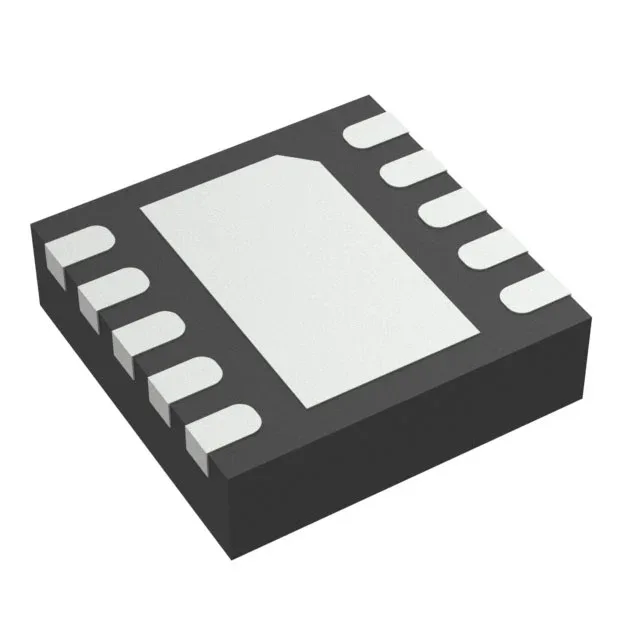
Texas Instruments TPS61029DRCR — DC-DC Power Modules

TPS61029DRCR Boost Converter, 1.8A Switch, 0.9V-5.5V

MPNTPS61029DRCR
Active

Texas Instruments TPS61029DRCR, Step-Up Boost Converter, Adjustable Output 1.8V to 5.5V, 1.8A Switch, 600kHz, Synchronous Rectification, 10-VFDFN Exposed Pad, -40°C to 85°C.

$2.5700Ref. price · indicative, final on quote
Independent supplier — new & surplus stockAuthenticity-screened · ESD-safe packingListing updated Jul 2026

Specifications

TPS61029DRCR specifications
ParameterValue
Output typeAdjustable
MountingSurface Mount
Voltage - input5.5V
Voltage - output5.5V
Voltage - output (Min (Fixed))1.8V
Output current1.8A (Switch)
Frequency - switching600kHz
I/O channels1
Operating temperature-40°C~85°C(TA)
PackageTape & Reel (TR); Cut Tape (CT)
FunctionStep-Up
TopologyBoost
Case10-VFDFN Exposed Pad
Output configurationPositive
Synchronous rectifierYes

Product details

Boost converter for battery-powered rails

The 600 kHz switching frequency allows the use of small inductors and ceramic capacitors, keeping the total solution footprint compact. Synchronous rectification improves efficiency at lower output voltages compared to a diode-based boost, which matters when the output is close to the input voltage.

Voltage rails and load budget

The 1.8 A switch current is the peak current the internal NMOS switch can handle. For a given output voltage and load, the input current will be higher than the output current by the boost ratio divided by efficiency. A 3.3 V output at 500 mA from a 1.5 V input, for example, draws roughly 1.2 A from the input — leaving headroom below the 1.8 A switch limit.

The datasheet layout recommendation calls for multiple vias under the pad to a ground plane.

Frequently asked questions

Is TPS61029DRCR compatible with 3.3 V input?

Yes. The output can be set to a higher voltage if needed, or the part can be configured as a pass-through if the input already matches the desired output.

What is the footprint of TPS61029DRCR?

The device is supplied in a 10-pin VSON package with an exposed thermal pad, measuring 3 mm x 3 mm (supplier device package 10-VSON). The PCB land pattern should follow the TI recommended layout for the 10-VSON package, which includes a thermal pad with vias to a ground plane.