0.9 V minimum input — why it matters for battery-powered designs
The TPS61020DRCR starts up and regulates from an input as low as 0.9 V, which means it can extract useful energy from a single alkaline or NiMH cell well past the point where most boost converters drop out. For a 1.5 V cell that sags to 1.0 V under load, this part keeps the output rail alive — that is the difference between a device that runs the battery flat and one that leaves 20 % of the energy on the table. The 1.5 A switch current rating sets the practical output power limit. At 3.3 V out from a 1.2 V input, duty cycle is around 64 %, so the switch handles roughly 2.4 A peak — the 1.5 A rating means you should budget output current around 600 mA to 800 mA in that scenario, depending on inductor ripple. If your load needs more, step up to a controller with an external FET.
600 kHz switching — inductor size vs. efficiency trade-off
The 600 kHz switching frequency is a middle ground: it allows a 4.7 µH to 10 µH inductor — small enough for a 3x3 mm VSON layout — without pushing switching losses so high that light-load efficiency suffers. For comparison, a 1 MHz boost would shrink the inductor further but increase gate-drive losses; a 300 kHz part would need a physically larger inductor for the same ripple current. That recovers 3 % to 5 % efficiency at moderate loads (100 mA to 500 mA) compared to a diode-rectified boost, and it eliminates the external diode from the BOM. The trade-off is a slightly higher quiescent current, but for continuous-operation designs the efficiency gain outweighs it.
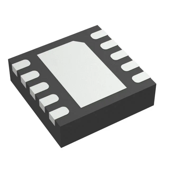
Package and thermal: 10-VSON with exposed pad
The pad is the primary heat path — without a solid thermal connection, the junction temperature rises quickly at the 1.5 A switch limit. The datasheet layout recommendation is worth following closely. For a design that sees 105°C ambient, you would need a different grade.
Cut Tape is also listed for smaller quantities. No official second source or pin-compatible alternate is recorded, so the BOM carries single-source risk — a factor to weigh if the design goes to high-volume production.