4 A output from a 3-17 V input rail
The TPS564252DRLR: The adjustable output goes from 0.6 V up to 10 V, so it can power a 1.2 V MCU core, a 3.3 V I/O bank, or a 5 V peripheral rail from the same BOM line. The 600 kHz switching frequency is a middle-ground choice: it keeps the inductor physically small — typically a 2.2 µH to 4.7 µH part — while staying below the point where switching losses dominate the efficiency curve. At light loads, the D-CAP3™ control scheme skips pulses to maintain regulation without the external compensation network that older architectures require. A synchronous rectifier is built in, replacing the usual freewheeling Schottky diode with a low-Rds(on) FET. This cuts the rectification loss by roughly 30-40 % compared to a diode-based buck at 4 A, which matters when the PCB has limited copper area for heat spreading.
SOT-563 footprint for tight layouts
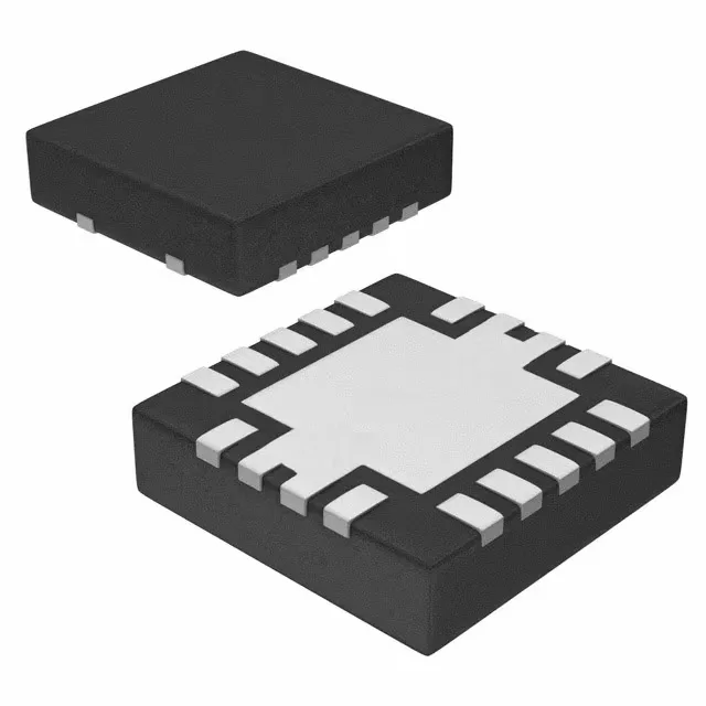
Housed in a SOT-563 package — a 1.6 mm × 1.6 mm body with 0.5 mm pitch leads — the TPS564252DRLR fits into space-constrained designs where a larger SOIC-8 or QFN would not route. Surface-mount assembly is standard for this package class.
Industrial temperature range — -40 to 125 °C junction
The 125 °C TJ ceiling means the part does not derate prematurely in a warm chassis.