3.5 A continuous output, 60 V input ceiling
The TPS54361DPRT delivers 3.5 A continuous output from a 4.5 V to 60 V input rail — this covers 12 V, 24 V, and 48 V industrial supplies, plus the cold-crank and load-dump transients on a 12 V automotive bus. The 60 V abs-max input means no external clamp is needed for 48 V telecom or 24 V truck systems that see 36 V during jump-start.
Switching frequency: 100 kHz to 2.5 MHz
The oscillator is programmable from 100 kHz to 2.5 MHz via a single resistor. At the low end, efficiency peaks and the inductor ripple current drops — useful when the load is near 3.5 A and the thermal budget is tight. At 2.5 MHz the inductor shrinks to a 4x4 mm footprint, but switching losses in the internal FET and the external Schottky diode (no synchronous rectifier — see below) raise the junction temperature. The trade-off is yours to set per the BOM's height and efficiency targets.
Split-rail topology for bipolar output rails
The split-rail (buck + inverting) topology lets the TPS54361DPRT generate a positive and a negative rail from a single positive input — useful for op-amp or ADC front-ends that need ±5 V or ±12 V from a 24 V supply. The output is adjustable from 0.8 V up to 60 V (the input voltage), set by a resistor divider on the FB pin.
No synchronous rectifier — external Schottky required
The TPS54361DPRT uses an external Schottky catch diode instead of an integrated synchronous FET. This adds one BOM line and a layout consideration — the diode's anode connects to PGND, cathode to the SW pin, and the loop from the input capacitor through the FET, inductor, and diode must be tight to keep radiated EMI below 30 MHz limits. The advantage is lower cost and no shoot-through risk; the trade-off is that the diode's forward drop (typically 0.45 V at 3 A) adds conduction loss that a synchronous part avoids. For a 3.5 A rail at 5 V output, the diode accounts for roughly 5-7% efficiency loss versus a synchronous design.
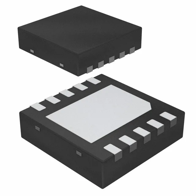
10-WSON exposed-pad package — thermal and layout notes
The 10-WSON (4x4 mm) package has an exposed thermal pad on the bottom. The datasheet recommends a 4x4 mm copper pour on the top layer, connected through at least four vias to the inner ground plane, to keep the junction temperature below 125°C at full load. The pad is electrically connected to PGND — no isolation slot needed. The 0.5 mm pitch on the signal pins means a 4-layer board is not mandatory, but a solid ground plane under the converter is strongly advised for thermal and EMI reasons.