Half-bridge driver for synchronous buck converters
The TPS51604QDSGRQ1 is a Texas Instruments half-bridge gate driver designed to drive two N-channel MOSFETs in a synchronous buck converter topology. It is qualified to AEC-Q100 Grade 1, meaning it is specified and tested for the -40°C to +125°C junction temperature range required in under-hood and chassis-mounted automotive electronics. The driver accepts a 4.5V to 5.5V supply rail, which is the bias voltage for the internal logic and the low-side gate drive. The high-side driver uses a bootstrap supply with an absolute maximum rating of 35V on the BST pin, so the converter's input voltage plus the bootstrap charging voltage must stay below that ceiling.
Switching speed and dead-time budget
The typical rise time is 30ns and the fall time is 8ns into the specified load. This asymmetric slew rate means the low-side MOSFET turns off faster than the high-side turns on, which helps prevent shoot-through but also sets a minimum dead-time the PWM controller must enforce. The controller's dead-time setting should exceed the turn-off propagation delay plus the fall time to guarantee break-before-make. The non-inverting input type means a logic high on the PWM input drives the high-side gate on; a logic low drives the low-side gate on.
Package and thermal design
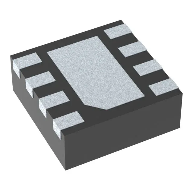
The device is housed in an 8-WSON package with a 2x2mm body and an exposed thermal pad (8-WFDFN). The supplier device package is designated 8-WSON (2x2). A layout that skips the thermal pad connection will raise the junction temperature above the 125°C limit under continuous high-frequency switching. Surface-mount assembly with the tape-and-reel or cut-tape packaging options.