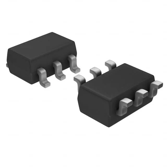
The Texas Instruments TPS3808G125QDBVRQ1 is a simple reset/power-on reset supervisor IC that monitors a single voltage rail and asserts a reset signal when the supply drops below the threshold. The reset output is active-low, open-drain, so it can be wire-ORed with other reset sources or pulled up to any voltage up to the absolute maximum of the output pin. The threshold is fixed at 1.16V, which makes it a natural fit for monitoring 1.2V or 1.8V core rails on automotive microcontrollers, FPGAs, or DSPs. One voltage monitored, one channel — no daisy-chaining needed for a single-rail system. The reset timeout is adjustable or selectable via an external capacitor on the CT pin, giving the designer control over the power-up sequencing delay.
The 1.16V threshold sits just below the nominal 1.2V supply, so the supervisor will assert reset when the rail droops about 40 mV below nominal. That's a tight window — good for catching brownouts early, but it means the power supply's load regulation and transient response need to keep the rail above 1.2V during normal operation, or you'll get nuisance resets. For a 1.8V rail, the margin is wider, but the threshold is still precise enough for most automotive-grade supplies.
Adjustable reset timeout — sizing the delay
The reset timeout is adjustable or selectable, meaning you set the delay with an external capacitor between the CT pin and ground. No fixed internal timer — you choose the reset pulse width to match the system's power-up sequence. Typical values range from a few milliseconds to several seconds, depending on the capacitor value. This is useful when the MCU or FPGA needs the core rail stable before releasing reset, or when multiple supervisors need staggered timing.
SOT-23-6 package — rework and layout notes
The SOT-23-6 is a surface-mount package with six leads on a 0.95 mm pitch. It's small enough for space-constrained automotive ECUs but still reworkable with a hot-air station — no hidden pads, no thermal slug. The small footprint means the PCB land pattern needs to match the recommended layout in the datasheet to avoid solder bridging between adjacent pins.