Why the AEC-Q100 grade matters for your power rail
That 150°C TJ ceiling is the under-hood / engine-compartment grade — the commercial TPS2553DBVR stops at 125°C and carries no AEC-Q report. If your BOM calls for the Q variant, the part has been through the production-part approval process (PPAP) and the qualification test flow that automotive OEMs require.
85 mOhm Rds(on) and the 1.5 A continuous rating
The typical on-resistance of 85 mOhm at 5 V input sets the conduction loss floor. At 1 A load the I²R drop is 85 mW — negligible in a SOT-23-6 package if the copper pour under the switch is adequate. The 1.5 A maximum output is the rated continuous current; the adjustable current-limit threshold lets you set the trip point below that to protect the downstream load or the trace width.
Protection set: adjustable limit, overtemperature, UVLO
Three fault protections are integrated: adjustable current limiting (set via an external resistor on the ILIM pin), overtemperature shutdown, and undervoltage lockout. The UVLO threshold is fixed internally — the switch turns off when the input drops below about 2.5 V, preventing the pass FET from operating in the linear region. The slew-rate-controlled turn-on limits inrush current into capacitive loads; the open-drain status flag asserts low when the switch is in current-limit or thermal-shutdown.
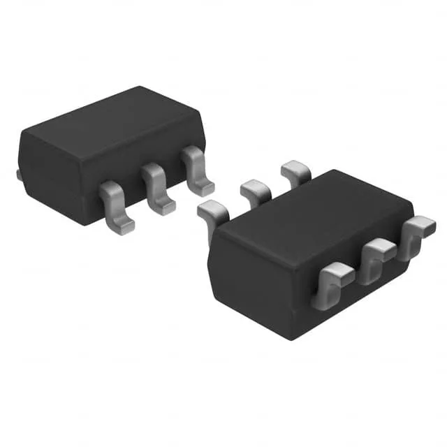
SOT-23-6 package — layout and thermal reality
The SOT-23-6 package has no exposed thermal pad. All heat is conducted through the leads into the PCB copper. For the 1.5 A maximum output at high ambient, the datasheet recommends a minimum of 0.5 square inches of 1-oz copper on the drain-connected pins (pins 5 and 6) to keep the junction temperature below the 150°C absolute maximum. The 0.50 mm lead pitch is standard for this package; a two-layer board with adequate copper area is sufficient for most loads up to 1 A.
It is a current-design-in part for automotive power-distribution applications.