85 mOhm Rds(on) — the conduction loss floor
The N-channel MOSFET output is driven by an internal charge pump, so no external Vcc supply is needed; the switch is controlled by a single On/Off logic input.
Adjustable current limit and fault protection
This matters when the load is a capacitive USB port or a motor that draws a start-up surge — the limit can be dialled just above the steady-state current to protect the cable and upstream supply. The part also includes overtemperature shutdown and undervoltage lockout; a status flag output asserts low when a fault (overcurrent or thermal) is active.
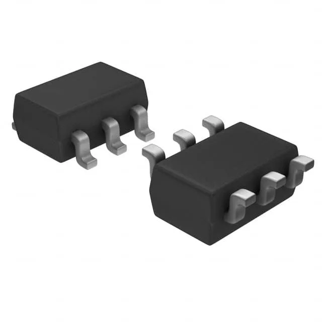
The SOT-23-6 package has a modest thermal footprint — the junction-to-ambient thermal resistance is around 200°C/W on a standard two-layer board, so at 1.5 A and 85 mOhm the self-heating adds roughly 40°C to the ambient. That leaves headroom in a 85°C ambient but pushes close to the limit at 125°C ambient; a design at full load in a hot environment should budget copper area on the drain pad.
Slew-rate controlled — limits inrush and EMI
The slew-rate controlled turn-on ramps the output voltage gradually, preventing the downstream capacitor from drawing a current spike that could trip the overcurrent limit or brown out the input rail. This is the feature that makes the TPS2552DDBVT a natural fit for USB port power switching, where the 120 µF or larger bulk capacitor on the VBUS line would otherwise cause a hard-start glitch.
Supply voltage and logic interface
The enable input is non-inverting and compatible with 1.8 V logic thresholds, so it can be driven directly by a 1.8 V or 3.3 V GPIO without a level shifter. The 1:1 input-to-output ratio means the switch is either fully on or fully off — no partial conduction.