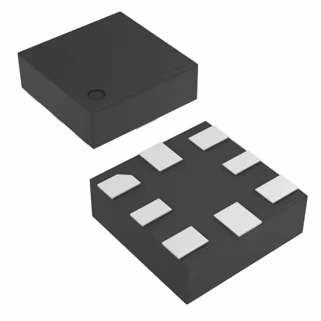
Texas Instruments TPS22933ARSER — Power Management (PMIC / Gate Driver)

TPS22933ARSER Source Selector Switch, 75mA, 2.5V-12V, 8-UQFN

MPNTPS22933ARSER
Active

Texas Instruments TPS22933ARSER, Source Selector Switch, P-Channel, 3:2 Input:Output, 75mA max output, 2.5V~12V supply, 65µs turn-on delay, 8-UQFN package, -40°C~85°C.

$0.4395Ref. price · indicative, final on quote
Independent supplier — new & surplus stockAuthenticity-screened · ESD-safe packingListing updated Jul 2026

Specifications

TPS22933ARSER specifications
ParameterValue
TypeSource Selector Switch
FET typeP-Channel
MountingSurface Mount
Supply voltage2.5V ~ 12V
Current - supply2 mA
Output current75mA
Operating temperature-40°C~85°C
PackageTape & Reel (TR); Cut Tape (CT)
ApplicationsHandheld/Mobile Devices
Case8-UFQFN
Delay time - ON65 µs
Delay time - OFF32 µs
Internal switchYes
Ratio - Input:Output3:2

Product details

Three-input, two-output power mux for portable rail selection

The Texas Instruments TPS22933ARSER is a P-channel source selector switch that routes one of three input supplies to two output rails, with a 3:2 input-to-output ratio. It is designed for handheld and mobile devices where the system must seamlessly switch between a battery, a USB VBUS, and an external adapter without back-feed between the sources. The internal P-channel FETs eliminate the need for external blocking diodes, reducing BOM count and forward voltage drop. With a supply range from 2.5 V to 12 V, it covers single-cell Li-ion through multi-cell or USB-C PD rails.

75 mA per output — enough for sensor rails and low-power peripherals

Each of the two outputs is rated for a maximum continuous current of 75 mA. This suits the part for power-gating sensor rails, low-power MCU I/O banks, Bluetooth/Wi-Fi module supplies, or audio codec rails — not for main processor or display backlight paths. The turn-on delay is 65 µs and the turn-off delay is 32 µs, which allows the downstream load to settle before the supply is switched. The 2 mA supply current is the quiescent draw of the control logic itself, not the load current.

Industrial temperature grade and 8-UQFN footprint

The 8-UQFN package (1.5 mm × 1.5 mm) requires a fine-pitch layout and a clean solder-paste stencil aperture for the thermal pad.

Active production — no immediate LTB risk

Frequently asked questions

Where can I buy TPS22933ARSER?

Buyers need a reliable source to purchase the exact part quickly and avoid counterfeit or long lead times.

What is the pinout of TPS22933ARSER?

Design engineers must verify pin compatibility for PCB layout before using the part.

Is TPS22933ARSER RoHS compliant?

Environmental compliance is mandatory for many designs and sourcing decisions.

What is the TPS22933ARSER equivalent?

Buyers or engineers may need a second-source alternative to mitigate supply risk or cost.

What is the price of TPS22933ARSER?

Sourcing buyers compare pricing across distributors to meet BOM cost targets.

Is TPS22933ARSER obsolete or end of life?

Brokers and buyers need lifecycle status to avoid supply disruption or redesign costs.