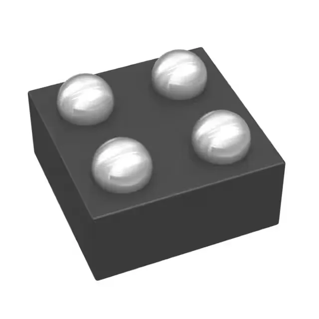
Texas Instruments TPS22930AYZVR — Power Management (PMIC / Gate Driver)

TPS22930AYZVR TI Power Switch, 35mOhm, 2A, 4-DSBGA

MPNTPS22930AYZVR
Active

Texas Instruments TPS22930AYZVR, P-channel general-purpose load switch, 35mOhm typical on-resistance, 2A max output, 1.4V to 5.5V load voltage, 4-DSBGA (0.88x0.88mm) package, slew-rate controlled, reverse current and UVLO protection.

$0.7600Ref. price · indicative, final on quote
Packaging4-XFBGA, DSBGA
RoHSROHS3 Compliant
Independent supplier — new & surplus stockAuthenticity-screened · ESD-safe packingListing updated Aug 2026

Specifications

TPS22930AYZVR specifications
ParameterValue
Input typeNon-Inverting
Output typeP-Channel
TypeGeneral Purpose
MountingSurface Mount
Voltage - load1.4V ~ 5.5V
Voltage - supply (Vcc (Vdd))Not Required
Output current2A
I/O channels1
InterfaceOn/Off
Operating temperature-40°C~85°C(TA)
PackageTape & Reel (TR); Cut Tape (CT)
FeaturesSlew Rate Controlled
Rds on35mOhm
Case4-XFBGA, DSBGA
Fault protectionReverse Current, UVLO
Output configurationHigh Side
Ratio - Input:Output1:1

Product details

35 mOhm P-channel load switch in 0.88 mm DSBGA

The TPS22930AYZVR is a single-channel, high-side P-channel load switch from Texas Instruments, part of the TPS22930 family. It handles a continuous output current up to 2 A with a typical on-resistance of 35 mOhm, making it a low-loss path for power rail gating in battery-powered or space-constrained designs. The input voltage range spans 1.4 V to 5.5 V, covering common logic and battery rails from 1.8 V through 5 V. No external Vcc supply is needed — the switch is self-powered from the load voltage.

Slew-rate control and fault protection

The slew-rate controlled turn-on limits inrush current into capacitive loads, preventing upstream supply droop during power-up. This is a key feature when the switch feeds a bank of decoupling capacitors on a sensor or RF module. Built-in fault protection includes reverse current blocking (the switch disconnects when Vout exceeds Vin) and undervoltage lockout (UVLO) that holds the output off until the input rail is stable. These protections reduce external component count in a power sequencing chain. The On/Off interface is non-inverting — a logic high on the enable pin turns the switch on.

DSBGA footprint and board integration

The part comes in a 4-bump DSBGA (0.88 x 0.88 mm) package — a 0.4 mm pitch wafer-level chip-scale package. The small footprint saves board area but requires a solder-mask-defined pad layout and a controlled reflow profile. The package is surface-mount only; no through-hole alternative exists in this family.

The base product number is TPS22930; the suffix AYZVR denotes the 4-DSBGA package and tape-and-reel packaging. Cut tape options are also available for prototyping.

Frequently asked questions

What are the key protection features of the TPS22930AYZVR?

The switch includes reverse current blocking (prevents backflow when output voltage exceeds input) and undervoltage lockout (UVLO) that keeps the output off until the input rail is above the UVLO threshold. These features simplify power sequencing and protect downstream circuitry.

Can I hand-solder the TPS22930AYZVR in a 4-DSBGA package?

It is possible with a fine-tip iron, flux, and steady hands, but the 0.88 x 0.88 mm DSBGA with 0.4 mm pitch bumps is better suited to reflow soldering. A hot-air station with a small nozzle or a toaster-oven reflow profile gives more reliable results. Use a stencil for solder paste if doing more than one or two boards.