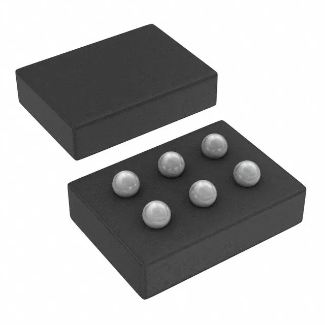
TPS22925CNYPHR

Texas Instruments

Texas Instruments TPS22925CNYPHR load switch, high-side, N-channel, 9.2 mOhm typical Rds(on), 3 A max output, 0.65 V to 3.6 V load range, DSBGA-6 package, -40°C to 105°C.

Texas Instruments TPS22925CNYPHR
Download datasheet (PDF)
[IN STOCK] In Stock: 3 pcs
$0.56/ pc

Volume pricing

Buy Now

MOQ 1 · Tape & Reel (TR); Cut Tape (CT) · RoHS · EIA-481 · DAP/DDP · T/T

Technical specifications

TPS22925CNYPHR specifications
Parameter / AttributeSpecification / Value
Input typeNon-Inverting
Output typeN-Channel
TypeGeneral Purpose
MountingSurface Mount
Voltage - load0.65V ~ 3.6V
Voltage - supply (Vcc (Vdd))Not Required
Output current3A
I/O channels1
InterfaceOn/Off
Operating temperature-40°C~105°C(TA)
PackageTape & Reel (TR); Cut Tape (CT)
FeaturesSlew Rate Controlled
Rds on9.2mOhm
Case6-XFBGA, DSBGA
Fault protectionReverse Current
Output configurationHigh Side
Ratio - Input:Output1:1

Technical details

9.2 mOhm on-resistance — what it buys the rail

The TPS22925CNYPHR: That on-resistance number is the headline spec: at 3 A output, conduction loss sits at roughly 83 mW at 25°C junction, which keeps the 6-DSBGA package cool enough to run without a heatsink in most board layouts.

Reverse current protection and slew rate control

Fault protection includes reverse current blocking — if the output rail stays high after the input drops, the switch prevents back-feed into the upstream supply. That matters for multi-rail systems where a downstream bulk cap holds charge longer than the input bus. The slew-rate-controlled turn-on limits inrush current during hot-plug or power sequencing, which avoids pulling the upstream regulator into current limit. The switch is non-inverting and uses a simple On/Off interface; no external Vcc/Vdd bias rail is required, so it can be driven directly from a GPIO.

The 6-DSBGA package requires a controlled SMT profile and a clean PCB surface finish.

TPS22925CNYPHR
[ALLOC] verified
Quote