18.3 mOhm Rds(on) at 2 A — the conduction loss floor
The TPS22924CYZPRB is a single-channel, high-side load switch from TI's TPS22924 family. Its headline spec is the 18.3 mOhm typical on-resistance, which at 2 A continuous output drops about 37 mV and dissipates roughly 73 mW — negligible for most board-level power gating, but worth checking against the DSBGA thermal budget if the switch sits near other hot components.
The load voltage range spans from 0.75 V (deep-sub-1 V core rails for modern FPGAs and SoCs) up to 3.6 V (3.3 V I/O and peripheral supplies). No separate Vcc/Vdd bias is required — the switch is self-powered from the input side, which simplifies the BOM for a single-rail power sequencer.
DSBGA-6 footprint — board area vs. layout discipline
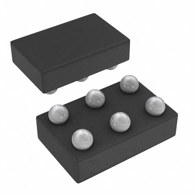
The 6-DSBGA package measures 1.39 x 0.89 mm — roughly the area of a 0402 resistor. The fine-pitch BGA demands a solder-mask-defined pad with a 0.25 mm via-in-pad for the centre output ball if routing under the part.
Slew-rate controlled with load discharge
The integrated slew-rate control limits inrush current when the switch turns on, preventing upstream rail droop. The load-discharge feature pulls the output to ground through an internal resistor when the switch is off — critical for preventing floating nodes on 1.8 V logic lines during power sequencing.
The non-inverting On/Off interface is 1.8 V logic-compatible, so it gates directly from a GPIO on a 1.8 V MCU or FPGA bank without a level shifter.
TI lists the TPS22924CYZPRB as Active. The base product number TPS22924 covers a family of load switches in different on-resistance and package variants; the CYZPRB suffix specifically identifies the 6-DSBGA, 2 A, slew-rate-controlled version with load discharge.