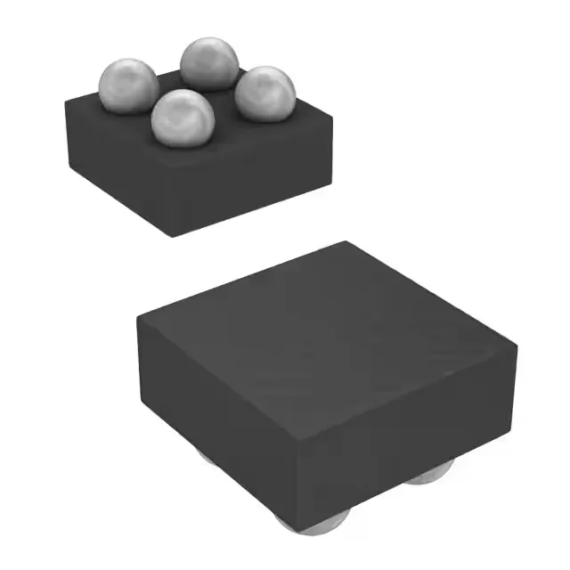
Texas Instruments TPS22916CNYFPR — Power Management (PMIC / Gate Driver)

TPS22916CNYFPR Power Switch – TI, 2 A, 5.5 V, DSBGA

MPNTPS22916CNYFPR
Active

Texas Instruments TPS22916CNYFPR, P-Channel load switch, 1:1 high-side, 0 V to 5.5 V load, 2 A max output, 200 mOhm typ Rds(on), slew-rate controlled, reverse current protection, 4-DSBGA package.

$0.6000Ref. price · indicative, final on quote
Packaging4-XFBGA, DSBGA
RoHSROHS3 Compliant
Independent supplier — new & surplus stockAuthenticity-screened · ESD-safe packingListing updated Aug 2026

Specifications

TPS22916CNYFPR specifications
ParameterValue
Input typeNon-Inverting
Output typeP-Channel
TypeGeneral Purpose
MountingSurface Mount
Voltage - load0V ~ 5.5V
Voltage - supply (Vcc (Vdd))1V ~ 5.5V
Output current2A
I/O channels1
Operating temperature-40°C~85°C(TA)
PackageTape & Reel (TR); Cut Tape (CT)
FeaturesSlew Rate Controlled
Rds on200mOhm
Case4-XFBGA, DSBGA
Fault protectionReverse Current
Output configurationHigh Side
Ratio - Input:Output1:1

Product details

Load-switch selection for 2 A rails

The TPS22916CNYFPR is a single-channel P-Channel load switch from Texas Instruments, designed for general-purpose high-side power gating up to 2 A continuous output. The load voltage range spans 0 V to 5.5 V. Slew-rate controlled turn-on limits inrush current into capacitive loads, which is the primary reason a designer picks this part over a discrete P-channel FET. Reverse current protection prevents back-feed when the output bus holds charge after the input drops — useful in hot-swap or OR-ing topologies.

Supply rails and control logic

The switch is controlled by a non-inverting input with a supply voltage (Vcc/Vdd) range of 1 V to 5.5 V. This means the enable logic threshold tracks the bias rail, not the load — a 1 V or 5.5 V GPIO can drive the EN pin directly. The 1:1 input-to-output ratio means one control line gates one power rail.

Package, footprint, and sourcing posture

The TPS22916CNYFPR is supplied in a 4-DSBGA package. The DSBGA is a chip-scale package with no exposed thermal pad; the primary heat path is through the solder balls into the PCB copper.

Frequently asked questions

What is the maximum current rating of TPS22916CNYFPR?

The maximum continuous output current is 2 A. The 200 mOhm typical on-resistance results in 0.8 W dissipation at full load — the DSBGA package relies on PCB copper for heat spreading.

Is TPS22916CNYFPR compatible with 3.3V logic?

Yes.