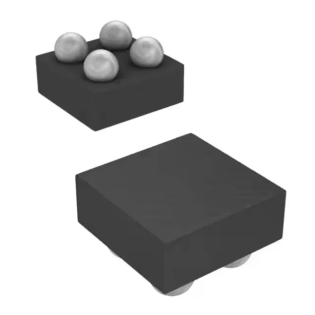
The TPS22916BYFPT is a single-channel, high-side load switch from Texas Instruments, built around a P-channel MOSFET with a typical on-resistance of 200 mOhm. It handles a continuous output current of 2 A across a load voltage range of 0 V to 5.5 V, making it a direct fit for 1.8 V, 2.5 V, 3.3 V, and 5 V rails without needing a level translator on the enable pin. The input supply (Vcc/Vdd) runs from 1 V to 5.5 V, so the same part can be driven by a 1.8 V GPIO or a 3.3 V logic output. The non-inverting input means a logic high turns the switch on — no inversion to account for in firmware. Slew-rate control limits the turn-on current surge, which prevents the input rail from dipping below the brown-out threshold of a co-located MCU or sensor. Reverse-current protection blocks back-feed from an output capacitor or a downstream rail when the switch is off — useful in power-sequencing schemes where multiple rails share a common output node.
Package and PCB integration
The supplier device package is 4-DSBGA. Hand soldering is not practical — the part is reflow-only, and the profile must stay within the JEDEC MSL-1 moisture sensitivity level (implied by the active ROHS3 compliance,). For 2 A continuous, a 1-oz copper pour of at least 200 mm² on the top layer is recommended to keep the junction below 85°C at 25°C ambient.
ROHS3 compliant. No direct replacement or pin-compatible second source is listed by TI; the TPS22916 family shares the same bump map across its variants, but the BYFPT suffix is specific to this package and temperature grade.