Texas Instruments TPS22916BLYFPR — Power Management (PMIC / Gate Driver)

TPS22916BLYFPR Load Switch, 5.5V 2A 60mOhm DSBGA

MPNTPS22916BLYFPR
Active

Texas Instruments TPS22916BLYFPR, general-purpose high-side load switch, 1 V to 5.5 V supply, 2 A continuous output, 60 mOhm typical Rds(on), 4-DSBGA package, -40°C to 85°C operating temperature.

$0.6600Ref. price · indicative, final on quote
Packaging4-XFBGA, DSBGA
RoHSNot applicable
Independent supplier — new & surplus stockAuthenticity-screened · ESD-safe packingListing updated Aug 2026

Specifications

TPS22916BLYFPR specifications
ParameterValue
Input typeInverting
Output typeP-Channel
TypeGeneral Purpose
MountingSurface Mount
Voltage - load1V ~ 5.5V
Voltage - supply (Vcc (Vdd))Not Required
Output current2A
I/O channels1
InterfaceOn/Off
Operating temperature-40°C ~ 85°C (TA)
PackageTape & Reel (TR) Cut Tape (CT)
FeaturesSlew Rate Controlled
Rds on60mOhm
Case4-XFBGA, DSBGA
Fault protectionReverse Current
Output configurationHigh Side
Ratio - Input:Output1:1

Product details

What this load switch does for a power rail

It handles up to 2 A continuous current with a typical on-resistance of 60 mOhm, which keeps the voltage drop under 120 mV at full load — relevant when the downstream regulator has tight headroom. The switch is controlled by a single On/Off logic input; the input type is inverting, so a logic low on the enable pin turns the output on. No separate Vcc supply is needed — the part is self-powered from the load voltage. The slew-rate controlled feature limits inrush current during turn-on, which reduces supply droop on a shared bus and avoids false resets on adjacent ICs.

Reverse-current protection — when it matters

The TPS22916BLYFPR includes reverse-current protection. If the output voltage rises above the input — for instance, during a power-source handoff or when a bulk capacitor holds the rail high after the input is removed — the switch blocks back-feed. This prevents downstream loads from powering upstream circuitry through the body diode, which could otherwise keep a bus alive unintentionally or damage a weak source.

Package and layout — the 4-DSBGA reality

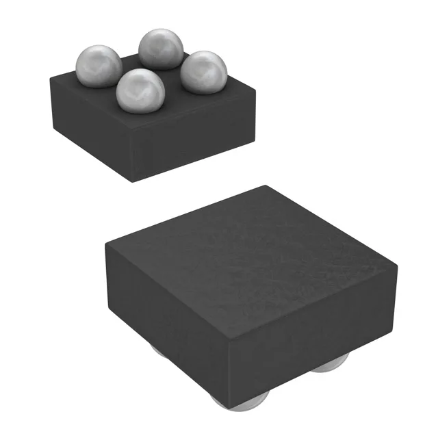
The part comes in a 4-bump DSBGA (4-XFBGA) package, supplier device package 4-DSBGA. The bump pitch is 0.5 mm; the overall body is approximately 0.8 mm x 0.8 mm. This is a wafer-level chip-scale package — no leads, no exposed thermal pad. The die attaches directly to the board, so the PCB landing pattern must match the TI-recommended footprint exactly. Solder mask defined pads are typical. For rework, hot air with a fine nozzle and low airflow is needed; the small mass heats quickly, so a gentle profile avoids lifting adjacent passives.

No external bias supply is needed, which simplifies the BOM.

It is a current TI product, listed as Active. The base product number is TPS22916; the suffix BLYFPR specifies the 4-DSBGA package and the reel/tape quantity.

Frequently asked questions

Is TPS22916BLYFPR compatible with 3.3V logic?

Yes. The enable input is inverting and the switch operates from 1 V to 5.5 V. A 3.3 V logic high on the enable pin will be seen as a logic high, turning the switch off. A 3.3 V logic low (ground) turns it on. The part does not require a separate Vcc supply, so the logic threshold tracks the load voltage.

Can TPS22916BLYFPR replace TPS22916B?

The TPS22916BLYFPR is a specific package and reel variant of the TPS22916 base product. The base product number TPS22916 is shared; the suffix BLYFPR denotes the 4-DSBGA package and tape/reel format. If the existing design uses a TPS22916 in a different package (e.g., SOT-23), the DSBGA footprint is not pin-compatible — the board layout must change. Electrically, the switch function and ratings are the same across the TPS22916 family.