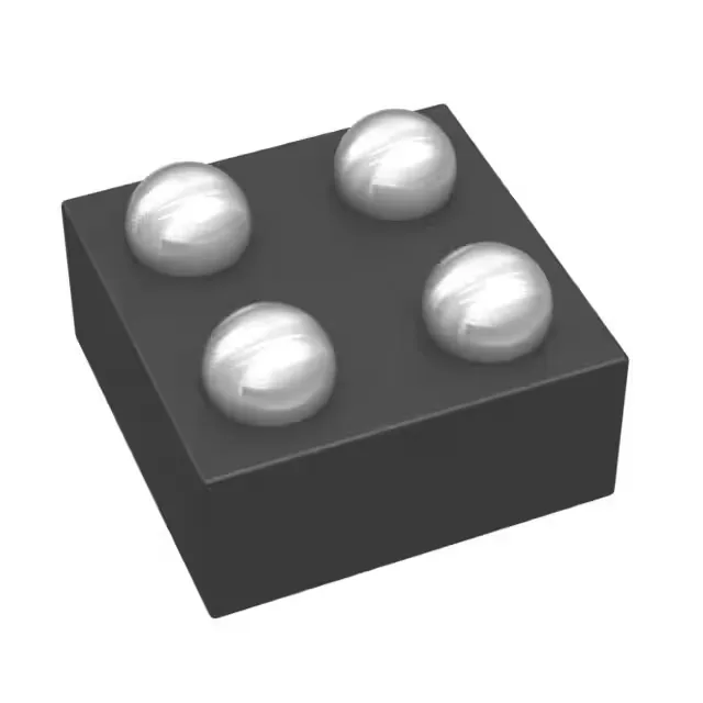
Texas Instruments TPS22915BYFPR — Power Management (PMIC / Gate Driver)

TPS22915BYFPR – TI 2A Load Switch, 37mOhm, DSBGA-4, Active

MPNTPS22915BYFPR
Active

Texas Instruments TPS22915BYFPR, 2 A load switch, 37 mOhm typical Rds(on), 1.05 V to 5.5 V load range, single N-channel high-side output, 4-bump DSBGA package, -40°C to 85°C operation.

$0.6000Ref. price · indicative, final on quote
Packaging4-XFBGA, DSBGA
RoHSROHS3 Compliant
Independent supplier — new & surplus stockAuthenticity-screened · ESD-safe packingListing updated Aug 2026

Specifications

TPS22915BYFPR specifications
ParameterValue
Input typeNon-Inverting
Output typeN-Channel
TypeGeneral Purpose
MountingSurface Mount
Voltage - load1.05V ~ 5.5V
Voltage - supply (Vcc (Vdd))Not Required
Output current2A
I/O channels1
InterfaceOn/Off
Operating temperature-40°C~85°C(TA)
PackageTape & Reel (TR); Cut Tape (CT)
FeaturesLoad Discharge, Slew Rate Controlled
Rds on37mOhm
Case4-XFBGA, DSBGA
Output configurationHigh Side
Ratio - Input:Output1:1

Product details

The TPS22915BYFPR is a single-channel, high-side N-channel load switch from Texas Instruments, rated for 2 A continuous output and a load voltage range of 1.05 V to 5.5 V. The 37 mOhm typical on-resistance sets the conduction loss: at 2 A, expect roughly 74 mV drop and 148 mW dissipation inside the package — manageable for the 4-DSBGA if the PCB copper carries the heat. The part includes load discharge and slew-rate control, which limits inrush current when the switch turns on and pulls the output to ground when off — useful for sequencing FPGA core rails or sensor supplies where a floating output could cause latch-up.

The load voltage spans 1.05 V to 5.5 V, covering 1.2 V, 1.8 V, 2.5 V, 3.3 V, and 5 V rails from a single device. The switch does not require a separate Vcc/Vdd supply; it is self-powered from the load input, simplifying the BOM by one rail.

Package and footprint — DSBGA placement reality

The 4-XFBGA, DSBGA package with a 4-bump array uses a 0.5 mm pitch typical for this family. The small bump diameter and tight pitch mean the stencil aperture and solder-paste volume must be controlled to avoid bridging or head-in-pillow defects.

Frequently asked questions

What is the exact Rds(on) of TPS22915BYFPR?

The typical Rds(on) is 37 mOhm. This is the on-resistance at nominal conditions; actual value increases with junction temperature per the normalised curve in the datasheet.

How does TPS22915BYFPR compare to TPS22915?

TPS22915 is the base product number. The BYFPR suffix indicates the 4-DSBGA package and reel packaging. The electrical specifications — 37 mOhm Rds(on), 2 A output, 1.05 V to 5.5 V range — are common across the TPS22915 family. The comparison is between package variants, not different silicon.