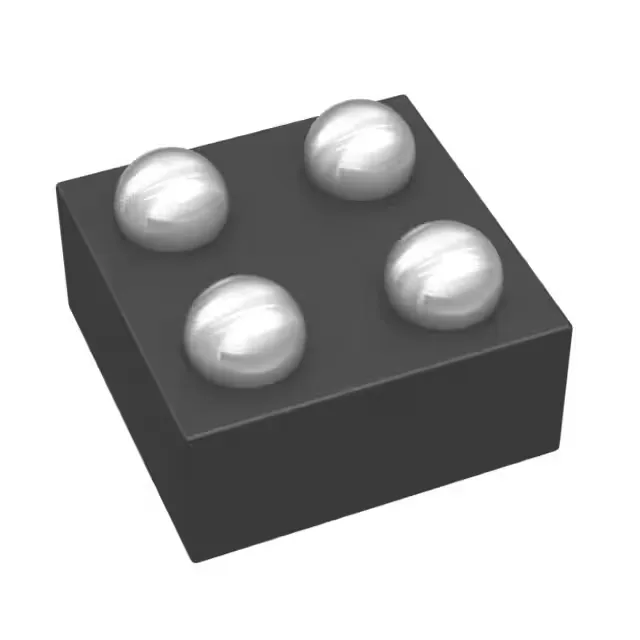
2 A load switch in a 0.88 mm² DSBGA
The TPS22910AYZVR is a single-channel P-Channel load switch from Texas Instruments, rated for 2 A continuous output across a 1.4 V to 5.5 V load range. Its 60 mOhm typical on-resistance keeps conduction losses low enough that the 4-DSBGA package (0.88x0.88 mm) can handle the current without a heatsink in most ambient conditions. The part integrates slew-rate control to limit inrush current on hot-plug or power-sequencing rails, and includes reverse-current blocking and undervoltage lockout — protections that save external Schottky diodes and supervisor ICs on the BOM.
Parametric deep-dive: on-resistance and protection
Rds(on) is specified at 60 mOhm typical — at 2 A load this yields 240 mW conduction loss, which the DSBGA's exposed die pad must sink to the PCB copper. The UVLO threshold ensures the switch stays off when the input rail droops below the minimum operating voltage, preventing the downstream load from seeing a partially enhanced FET. Reverse-current protection blocks back-feed from output to input when the load voltage exceeds the supply — useful in multi-rail systems where one rail powers down before another.
The 4-DSBGA (0.88x0.88 mm) package has a 0.50 mm ball pitch — the centre two balls are the output and input power, the outer two are the enable and ground. The small footprint demands a 4-layer PCB with micro-vias for thermal relief; the exposed die pad on the bottom side must connect to a copper pour with at least 4 thermal vias to keep junction temperature below 125°C at 2 A.
Lifecycle and compliance posture
It is ROHS3 Compliant and lead-free — the DSBGA package uses SAC305 solder balls, compatible with standard lead-free reflow profiles. The base product number TPS22910 covers the family; the YZV suffix denotes the 4-DSBGA package. For a pin-compatible alternative, the TPS22910AYZVR is the only variant in this package — no direct second-source exists from other manufacturers.