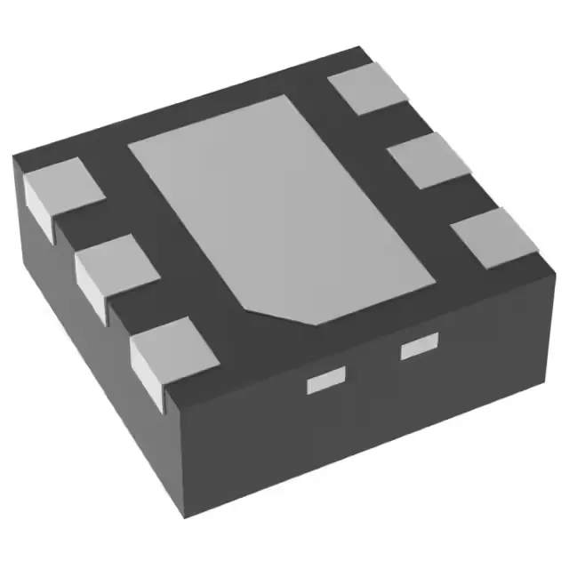
79 mOhm N-channel load switch for 2.7 V to 18 V rails
The TPS22810DRVR: It handles continuous loads up to 3 A across a supply range of 2.7 V to 18 V. The switch is controlled by a single On/Off logic input and does not require a separate Vcc/Vdd bias rail — it powers itself from the load voltage. Built-in features include slew-rate controlled turn-on to limit inrush current into capacitive loads, and an active load-discharge path that pulls the output to ground when the switch is disabled. Fault protection covers over-temperature shutdown and undervoltage lockout (UVLO), reducing the need for external monitor circuitry.
3 A continuous current and the thermal budget
At 3 A and 79 mOhm, the conduction loss is I²R = 0.71 W typical. The 6-WSON (2x2 mm) package with exposed pad relies on the PCB copper area for heat spreading — the datasheet's RθJA figure assumes a minimum pad size and via pattern. For sustained 3 A operation at 105°C ambient, the layout engineer must allocate a thermal land on the bottom layer with thermal vias; otherwise the junction temperature climbs above the 125°C absolute maximum. It does not carry AEC-Q100 automotive qualification, so it is not rated for under-hood or chassis-domain applications.
Load discharge and slew-rate control — why they matter
The load-discharge feature pulls the output to ground through an internal resistor when the switch is turned off. Without it, a downstream capacitive load holds its voltage and can back-feed the supply rail or cause undefined logic states during power sequencing. The slew-rate control limits the output voltage rise time, which directly caps the inrush current into the load capacitor — critical when the switch feeds a bank of bulk decoupling capacitors on a 12 V rail.