Active production — what it means for your BOM
The TMS5703137CGWTQEP: ROHS3 compliant — no exemption-based paperwork to manage for EU or similar restricted-material markets.
Core and memory headroom for safety-rated control
Built around the ARM Cortex-R4F core, a 16/32-bit lockstep architecture designed for functional-safety applications up to ASIL D / SIL 3. The 180 MHz clock delivers the throughput for real-time control loops with interrupt latency in the tens of nanoseconds. 3 MB of on-chip flash (3M x 8) and 256K x 8 of RAM leave headroom for a full AUTOSAR stack or a safety-critical application with multiple communication stacks and diagnostic routines — no external memory required for most mid-complexity ECUs.
Peripheral set and connectivity mix
Connectivity covers CANbus, FlexRay, Ethernet, along with I²C, SPI, SCI, UART/USART, and MibSPI — enough to bridge between a vehicle backbone (CAN/FlexRay) and a high-speed diagnostic or backbone link (Ethernet). The ADC array provides 16 x 12-bit and 24 x 12-bit channels, suitable for monitoring multiple analog sensor inputs (current, voltage, temperature) in a motor-drive or battery-management context. On-chip peripherals include DMA, POR, PWM, and WDT — the watchdog and POR are essential for safety-rated systems that must detect and recover from code hangs or brownout conditions without external supervisor ICs.
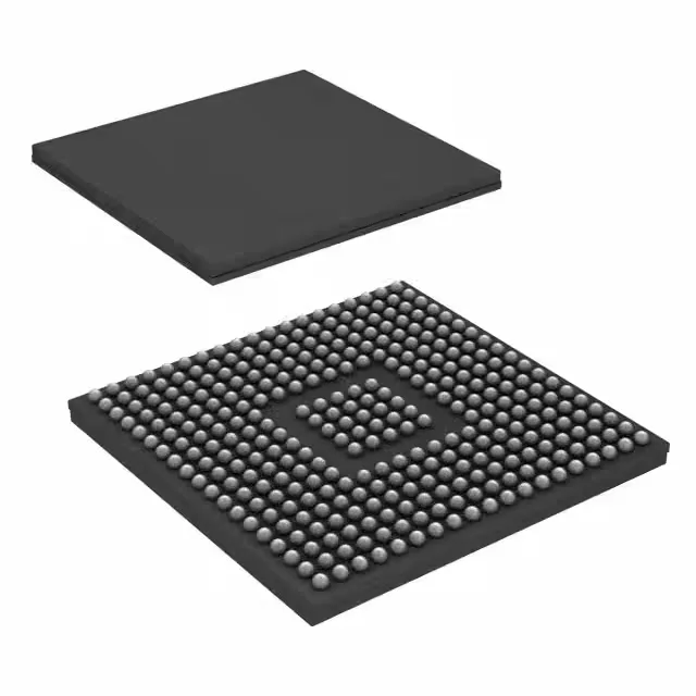
Supplied in a 337-ball NFBGA (16x16 mm) — the 0.8 mm ball pitch allows a 4-layer PCB with via-in-pad for decoupling, though a 6-layer stack-up gives cleaner power delivery for the 1.14 V to 1.32 V core supply.