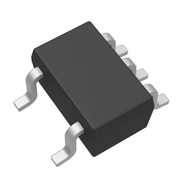
Texas Instruments TLV9151IDCKR — Interface & Transceivers

Texas Instruments TLV9151IDCKR Op-Amp, 4.5 MHz, SC-70-5

MPNTLV9151IDCKR
End of Life

Texas Instruments TLV9151IDCKR general-purpose op-amp, single circuit, 4.5 MHz gain bandwidth, 21 V/µs slew rate, rail-to-rail output, SC-70-5 package, tape and reel.

$0.92Ref. price · indicative, final on quote
Packaging5-TSSOP, SC-70-5, SOT-353
RoHSNot applicable
Independent supplier — new & surplus stockAuthenticity-screened · ESD-safe packingListing updated Aug 2026

Specifications

TLV9151IDCKR specifications
ParameterValue
Output typeRail-to-Rail
MountingSurface Mount
Amplifier typeGeneral Purpose
Voltage - input offset125 µV
Voltage - supply span2.7 V
Current - supply560µA
Current - input bias10 pA
Current - output (Channel)75 mA
Operating temperature-40°C ~ 125°C (TA)
Gain bandwidth product4.5 MHz
PackageTape & Reel (TR); Cut Tape (CT)
Slew rate21V/µs
Case5-TSSOP, SC-70-5, SOT-353
Number of circuits1

Product details

What the 4.5 MHz gain-bandwidth means for your signal chain

The TLV9151IDCKR: This combination means the op-amp can handle small-signal amplification up to about 4.5 MHz at unity gain, while the slew rate supports large-signal swings up to roughly 1.5 MHz before distortion sets in — useful for audio processing, sensor conditioning, or ADC driver stages where bandwidth matters.

Input bias current is just 10 pA typical, making this op-amp suitable for high-impedance sources like photodiodes or pH probes where bias current errors would otherwise dominate the offset budget. Input offset voltage is 125 µV typical, providing adequate DC accuracy for most general-purpose signal chains without requiring external trimming.

Temperature grade and package for real-world deployment

The SC-70-5 package occupies roughly 2.0 mm × 2.1 mm of board area — a space-saving footprint for multi-channel designs where PCB real estate is tight.

Output drive and load considerations

The output can source or sink 75 mA typical, which is enough to drive the analog input of a successive-approximation ADC directly, or to bias a small LED indicator. For heavier loads, an external buffer stage is recommended to avoid thermal stress on the output stage at elevated temperatures.

Frequently asked questions

How does TLV9151IDCKR compare to TLV9351IDCKR?

The TLV9351IDCKR is a close sibling with a slightly lower gain-bandwidth product (3.5 MHz vs 4.5 MHz) and a higher typical input offset voltage (350 µV vs 125 µV). Both share the same SC-70-5 footprint, supply range, and industrial temperature grade, so the TLV9151IDCKR offers better AC performance and DC precision for the same board layout.

How do I get current pricing and availability for TLV9151IDCKR?

Submit an RFQ through this listing.