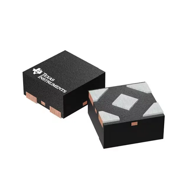
Texas Instruments TLV9061IDPWR — Logic ICs

TI TLV9061IDPWR CMOS Op-Amp, 10 MHz, Rail-to-Rail

MPNTLV9061IDPWR
End of Life

Texas Instruments TLV9061IDPWR, single CMOS rail-to-rail op-amp, 10 MHz gain-bandwidth, 6.5 V/µs slew rate, 1.8 V to 5.5 V supply, 0.5 pA input bias, -40 to 125°C, 5-X2SON (0.8x0.8 mm) package.

$0.97Ref. price · indicative, final on quote
Packaging5-XFDFN Exposed Pad
StockContact for availability
MOQ1 pcs
  • 100% new & originalTraceable channels only — no refurbs, no pulls, no remarked parts.
  • Date & lot codes on quoteStated per line before you commit; label photos on request.
  • MSL-compliant ESD packingMoisture-sealed bags with indicator cards; reels photo-verified.
  • PayPal buyer protectionPay by T/T, PayPal or Payoneer — card payments covered end to end.

Specifications

TLV9061IDPWR Technical Specifications
ParameterValue
Output typeRail-to-Rail
Mounting typeSurface Mount
Amplifier typeCMOS
Voltage - input offset300 µV
Voltage - supply span5.5 V
Current - supply538µA
Current - input bias0.5 pA
Current - output (Channel)50 mA
Operating temperature-40°C ~ 125°C (TA)
Gain bandwidth product10 MHz
PackageTape & Reel (TR); Cut Tape (CT)
Slew rate6.5V/µs
Case5-XFDFN Exposed Pad
Number of circuits1

Product details

10 MHz CMOS op-amp in a 0.8 mm² package

The rail-to-rail output stage maximizes dynamic range at low supply voltages. With an input bias current of 0.5 pA, it is well suited for high-impedance signal conditioning — photodiode transimpedance amplifiers, pH electrode buffers, or piezoelectric charge integrators — where bias current error would otherwise dominate the offset budget.

The 1.8 V minimum supply span means the TLV9061IDPWR can run directly from a single Li-ion cell or a 1.8 V logic rail without a boost converter.

Package and footprint — 5-X2SON with exposed pad

The TLV9061IDPWR is supplied in a 5-lead X2SON package measuring 0.8 mm × 0.8 mm (supplier device package 5-X2SON). The exposed thermal pad aids heat transfer to the PCB; a via stitch under the pad is recommended for continuous operation near the 50 mA output current limit at elevated temperature. The small footprint suits space-constrained designs such as handheld instruments, wearable medical patches, and compact IoT edge nodes.

Frequently asked questions

What is the input bias current of TLV9061IDPWR?

The input bias current is 0.5 pA typical, thanks to the CMOS input stage. This ultra-low bias is critical for high-impedance sensor interfaces where even nanoamp-level leakage would introduce unacceptable offset errors.

Is TLV9061IDPWR suitable for battery-powered devices?

Yes. The 1.8 V minimum supply allows direct operation from a single Li-ion cell, and the 538 µA quiescent current per channel supports extended battery life in portable and wireless sensor applications. The rail-to-rail output also preserves signal swing at low supply voltages.

What is the recommended alternate for TLV9061IDPWR if it is out of stock?

A close functional alternate is the TLV9351IDCKR, a single general-purpose rail-to-rail op-amp in a similar package. Note the TLV9351IDCKR has a 3.5 MHz gain-bandwidth and 20 V/µs slew rate — slower small-signal bandwidth but faster large-signal response. Verify the trade-off against your application's bandwidth and settling requirements before substituting.