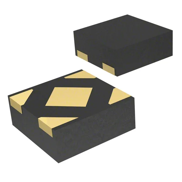
Package and board-fit — 4-X2SON with exposed pad
The TLV71333PDQNR is a 150 mA fixed-output LDO in a 4-X2SON package measuring 1x1 mm (supplier device package 4-X2SON). The exposed pad underneath is the primary thermal path — the board layout must connect it to a copper pour or via array to keep junction temperature within the -40 to 125 °C operating range. This is a single-output positive regulator with a fixed 3.3 V output. The enable pin lets you gate the output for sequenced power rails or low-power sleep modes — pulling it low drops the quiescent current from the 75 µA typical figure to near zero.
PSRR across frequency — where it matters for noise-sensitive rails
PSRR is specified at 70 dB at 100 Hz, rolling off to 55 dB at 1 MHz. That 55 dB floor at 1 MHz is the figure that matters for a rail feeding an RF or high-speed ADC front-end — switching regulator ripple at that frequency is attenuated by roughly 560x, not the 3000x the 70 dB figure suggests. If your load draws switching noise above 1 MHz, the attenuation drops further; a post-filter LC stage ahead of the LDO input may be needed. Maximum dropout voltage is 0.54 V at the full 150 mA load. With a 5.5 V max input, the headroom is generous for a 3.3 V output — the part runs cool even at full current as long as the input is not pushed to the ceiling.
Protection set and quiescent draw
The protection block includes over-current, over-temperature, reverse polarity, short-circuit, and under-voltage lockout (UVLO). The reverse polarity protection is notable for a small LDO — it saves an external Schottky on the input if the supply is ever wired backwards, though the reverse current path still depends on the input source impedance. UVLO holds the output off until the input rises above the threshold, preventing the downstream load from seeing a brown-out voltage on startup. Quiescent current is 75 µA typical. This is not an ultra-low-Iq part for always-on battery applications — that range starts below 1 µA — but 75 µA is reasonable for a general-purpose LDO powering a sensor or MCU that spends most of its time in active mode. The enable pin can cut that to near zero when the rail is not needed.